Shift register

a technology of shift register and shift register, which is applied in the direction of static storage, digital storage, instruments, etc., can solve the problems of tb>6/b> being erroneously operated, the bias temperature stress characteristic of the transistor,

Active Publication Date: 2005-10-06
LG DISPLAY CO LTD
View PDF3 Cites 188 Cited by
  • Summary
  • Abstract
  • Description
  • Claims
  • Application Information

AI Technical Summary

Problems solved by technology

However, the amorphous silicon thin film transistor has a bias temperature stress characteristic in which it operates erroneously due to bias stress when a direct current (DC) voltage is continuously supplied to the gate terminal thereof in a high temperature operation.
Accordingly, the conventional shift register has a problem in that, when it is operated at a high temperature, the sixth NMOS transistor T6 is erroneously operated due to gate bias stress.

Method used


Image

  • Shift register
  • Shift register
  • Shift register

Examples


first embodiment

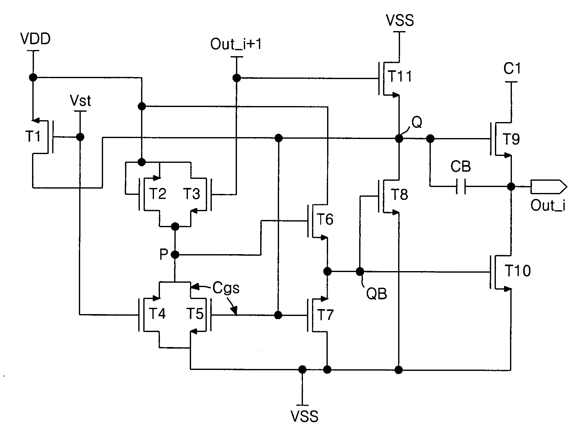
[0052]FIG. 4 is a detailed circuit diagram of one stage in a shift register according to the present invention, and FIG. 5 shows driving waveforms thereof.

[0053] Referring to FIG. 4, the stage of the shift register includes an output buffer having a ninth NMOS transistor T9 for outputting a first clock signal C1 to an output line under control of a Q node and a tenth NMOS transistor T10 for outputting a low-level driving voltage VSS to the output line under control of a QB node, a pre-charger having a first NMOS transistor T1 for pre-charging the Q node, a first controller having second to seventh NMOS transistors T2 to T7 for controlling the QB node, and a second controller having eighth and eleventh NMOS transistors T8 and T11 for controlling the Q node.

[0054] The ninth NMOS transistor T9 of the output buffer is connected between the input line of the first clock signal C1 and the output line of the stage to be controlled by the Q node, and the tenth NMOS transistor T10 is connec...

second embodiment

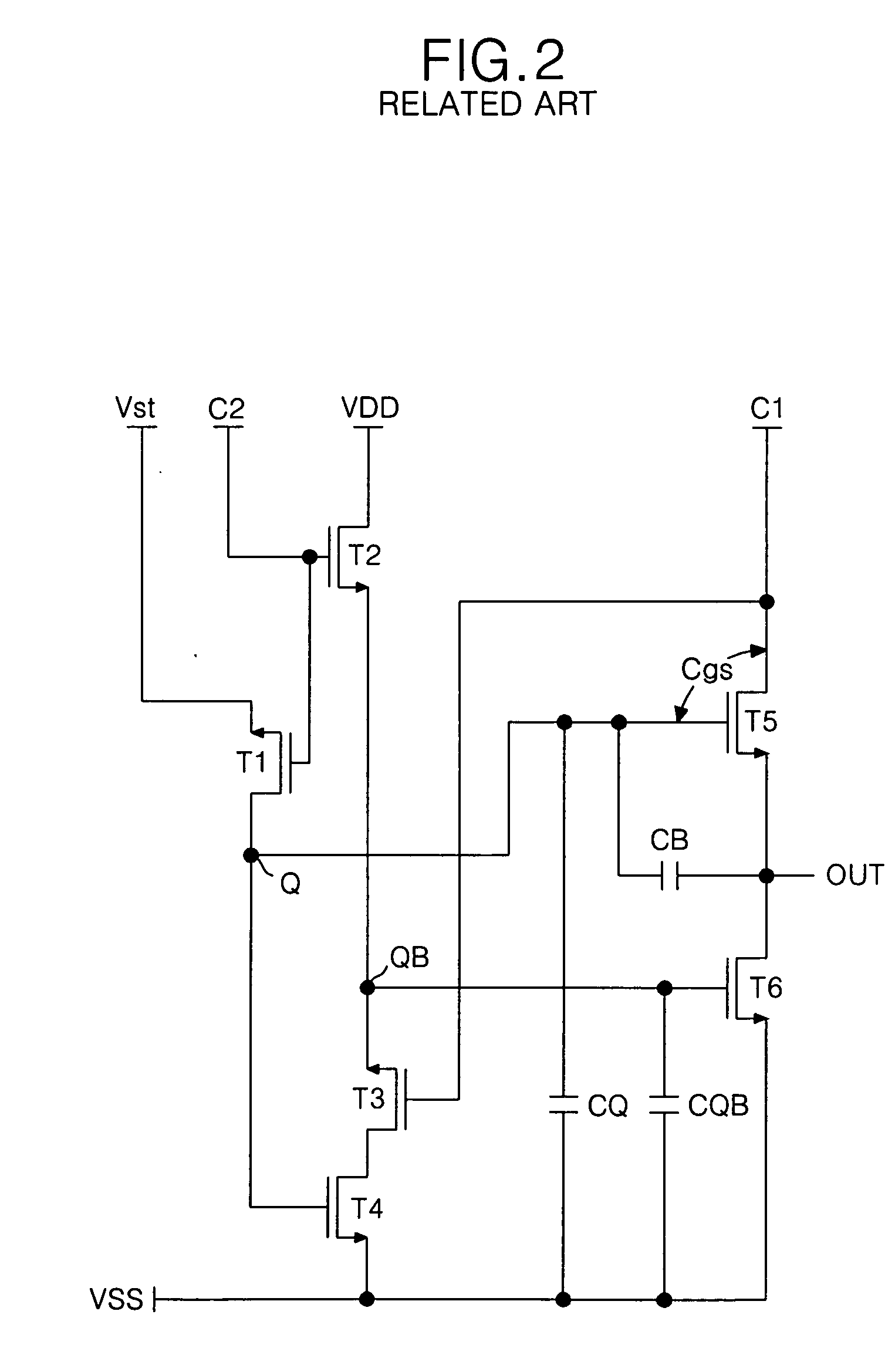
[0065] In order to solve the above-mentioned problem, a shift register according to the present invention will be described below.

[0066]FIG. 6 is a detailed circuit diagram of one stage in a shift register according to a second embodiment of the present invention, and FIG. 7 is a driving waveform diagram of the stage shown in FIG. 6.

[0067] Referring to FIG. 6, the shift register includes an output buffer having a fifth NMOS transistor T5 for outputting a clock signal C1 to an output line under control of a Q node and sixth and seventh NMOS transistors T6 and T7 for outputting a low-level driving voltage VSS to the output line under control of QB1 and QB2 nodes, a Q node controller having first and second NMOS transistors T1 and T2 and twelfth and thirteenth NMOS transistors T12 and T13 for controlling the Q node, a QB node controller having third and fourth NMOS transistors T3 and T4 for controlling a QB node, a QB1 node controller having eighth and ninth NNOS transistors T8 and T9...


PUM


Abstract

An output buffer in each stage of a shift register applies a first clock signal to an output line under control of a first node and a second driving voltage to the output line under control of second and third nodes. A first node controller controls the first node using a start pulse and an output signal of the next stage. A second node controller selectively applies a voltage at a fourth node and the second driving voltage to the second node under control of the first and second clock signals. A third node controller applies the voltage at the fourth node and the second driving voltage to the third node opposite to the second node. A fourth node controller controls the fourth node such that the fourth node has a voltage opposite to the first node using a voltage at the first node and the first driving voltage.

Description

[0001] This application claims the benefit of Korean Patent Application No. P2004-21987 filed in Korea on Mar. 31, 2004, which is hereby incorporated by reference. BACKGROUND [0002] 1. Field of the Invention [0003] This invention relates to a driving circuit for a liquid crystal display, and more particularly to a shift register employing an amorphous silicon thin film transistor. [0004] 2. Description of the Related Art [0005] Generally, a liquid crystal display (LCD) used as a display device for a television or a computer controls light transmittance of a liquid crystal using an electric field to thereby display a picture. To this end, the LCD includes a liquid crystal display panel having liquid crystal cells arranged in a matrix type, and a driving circuit for driving the liquid crystal display panel. [0006] In the liquid crystal display panel, gate lines and data lines are arranged to intersect each other. The liquid crystal cell is positioned at each area defined by intersecti...

Claims


Application Information

Patent Timeline
Patent Type & Authority Applications(United States)
IPC IPC(8): G09G3/36G11C19/00G11C19/28
CPCG11C19/00G11C19/28G11C19/184G09G3/36
Inventor MOON, SU HWAN
Owner LG DISPLAY CO LTD
Why Eureka
Try Eureka