Shift registrer and driving method thereof

a technology of shift register and shift register, which is applied in the direction of pulse technique, counting chain synchronous pulse counter, identification means, etc., can solve the problems of significant error in the operation of the lcd device, increase in the output voltage vout, and paralyze the output voltage cgd and cgs

a technology of shift register and shift register, which is applied in the direction of pulse technique, counting chain synchronous pulse counter, identification means, etc., can solve the problems of significant error in the operation of the lcd device, increase in the output voltage vout, and paralyze the output voltage cgd and cgs

US20050220263A1Inactive Publication Date: 2005-10-06LG DISPLAY CO LTD

Image

  • Shift registrer and driving method thereof
  • Shift registrer and driving method thereof
  • Shift registrer and driving method thereof

Examples


Embodiment Construction

[0039] Reference will now be made in detail to the preferred embodiments, examples of which are illustrated in the accompanying drawings.

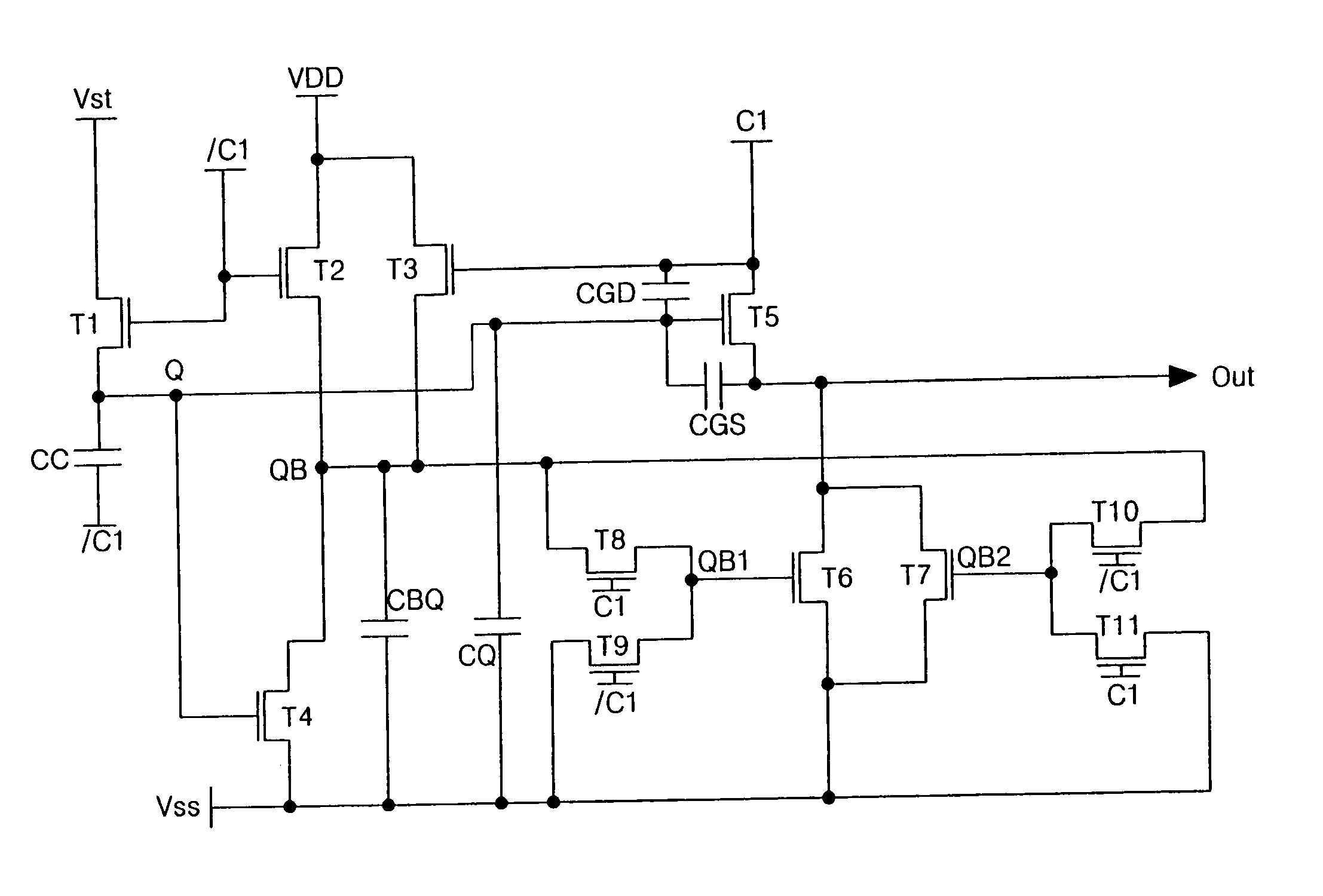
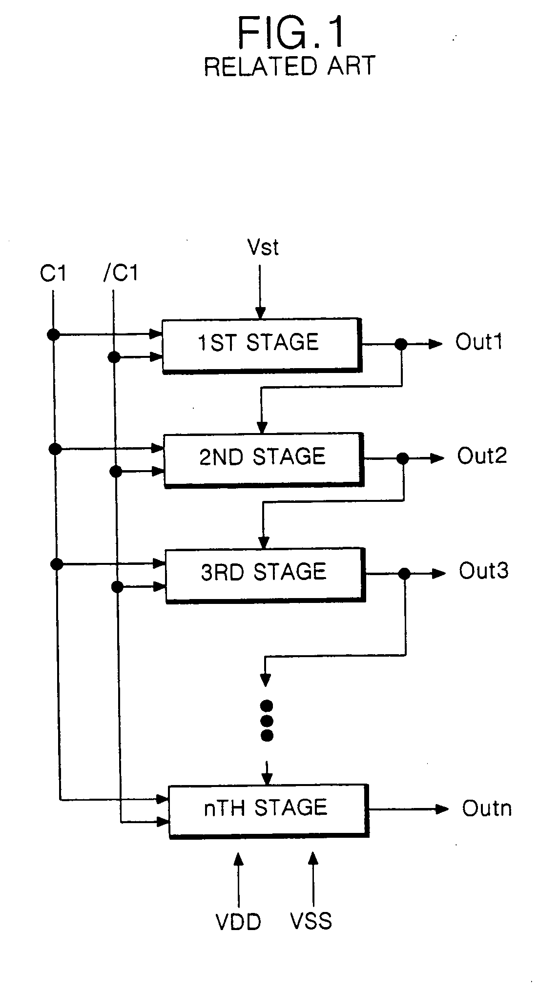
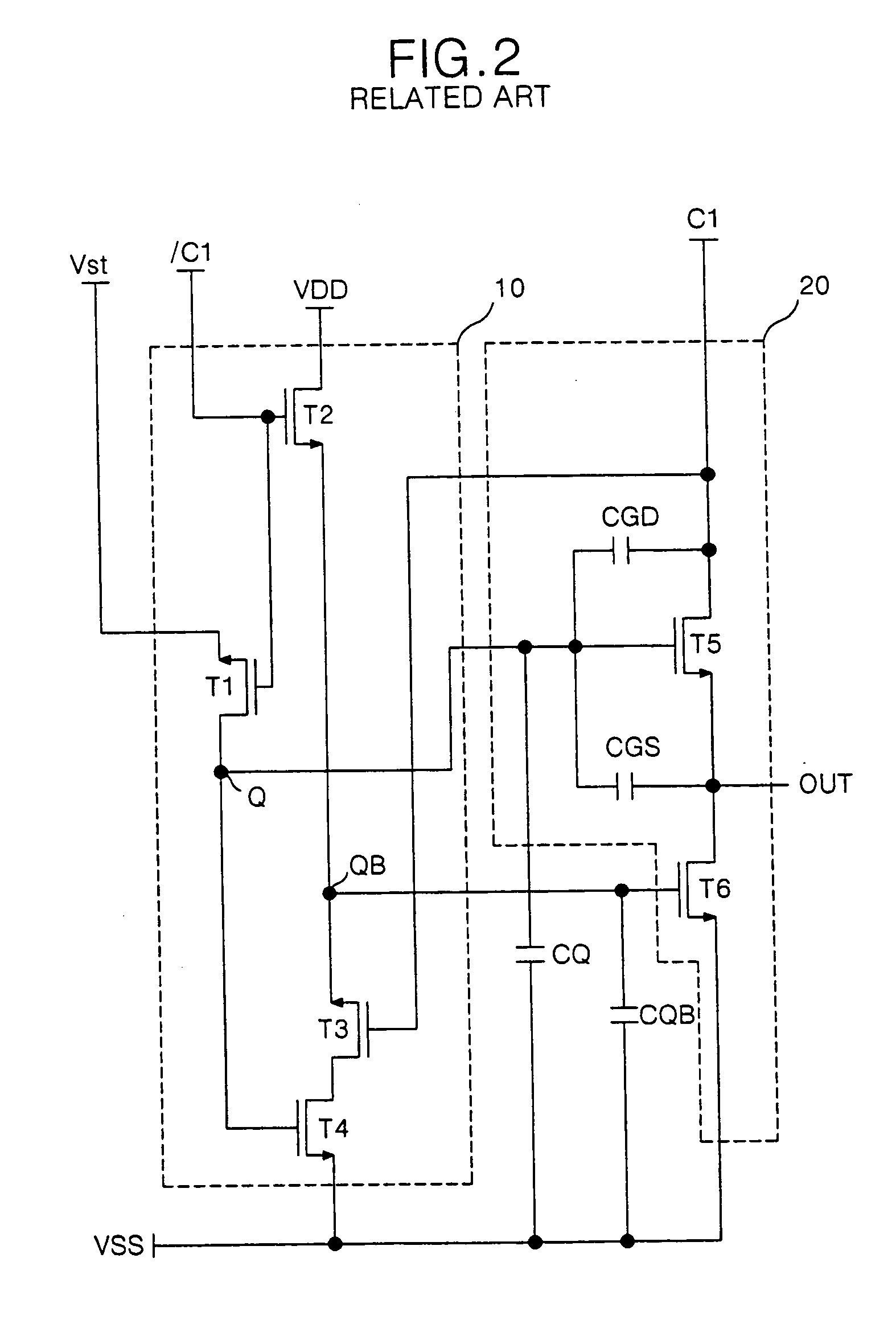
[0040]FIG. 4 is a circuit diagram showing an output portion of one stage of a shift register according to an embodiment of the present invention and FIG. 5 is a driving waveform diagram of the stage shown in FIG. 4. In FIG. 4, a stage of a shift register may include an output buffer 30 having a fifth transistor T5 for outputting a clock signal C1 to a output line OUT under the control of a first node Q, and a sixth transistor T6 for outputting a low-level driving voltage VSS to the output line OUT under the control of a second node QB. The fifth T5 may be a pull-up transistor and may include a NMOS transistor. In addition, the sixth transistor T6 may be a pull-down transistor and may include a NMOS transistor. A source terminal of the fifth transistor T5 may be connected to a drain terminal of the sixth transistor T6. Because the fifth transistor ...


PUM

PropertyMeasurementUnit
driving voltageaaaaaaaaaa
capacitanceaaaaaaaaaa
transition voltageaaaaaaaaaa

Abstract

A shift register having a plurality of stages for shifting a start pulse and outputting a shifted start pulse to a next stage, each of the plurality of stages includes a pull-up transistor controlled by a first node to apply a first clock signal to an output line, a first pull-down transistor controlled by a second node to apply a first driving voltage to the output line, a controller for controlling the first and second nodes, and a compensating capacitor connected between the first node and an input line of a second clock signal, the second clock signal being different from the first clock signal.

Description

[0001] The present application claims the benefit of Korean Patent Application No. P2004-21986 filed in Korea on Mar. 31, 2004 and Korean Patent Application No. P2004-30337 filed in Korea on Apr. 30, 2004, which are hereby incorporated by reference. BACKGROUND OF THE INVENTION [0002] 1. Field of the Invention [0003] This invention relates to a driving circuit for a liquid crystal display, and more particularly, to a shift register employing an amorphous silicon thin film transistor that prevents a voltage at a node, which controls an output buffer, from being varied due to a parasitic capacitor of the thin film transistor. [0004] 2. Discussion of the Related Art [0005] In general, liquid crystal display (LCD) devices are used in televisions, computers or portable devices. LCD devices use the optical anisotropy and polarization properties of liquid crystal molecules to generate a desired image. In particular, liquid crystal molecules can be aligned in a specific orientation, which ca...

Claims


Application Information

Patent Timeline
06 Oct 2005
Publication
US20050220263A1
IPC
G02F1/133; G09F9/35; G09G3/20; G09G3/36; G11C19/00; G11C19/18; G11C19/28; H03K5/13; H03K5/15; H03K17/687; H03K23/44
CPC
G11C19/00; G11C19/28; G11C19/184; G09G3/3677; G09G3/3688; H03K5/15093
Inventors
MOON, SU HWAN