Bonded three dimensional metal laminate structure and method

a three-dimensional, metal laminate technology, applied in the direction of coupling device details, coupling device connection, coupling protective earth/shielding arrangement, etc., can solve the problems of increasing the number of miniaturized connectors, the manufacturing of metallized housings, and the weak thin walled construction. achieve the effect of economic structur

Inactive Publication Date: 2005-10-06
TE CONNECTIVITY CORP
View PDF14 Cites 17 Cited by
  • Summary
  • Abstract
  • Description
  • Claims
  • Application Information

AI Technical Summary

Benefits of technology

[0007] It would be desirable to provide an economical structure for electrical connectors which avoids these and other issues.

Problems solved by technology

Manufacturing the metallized housings, however, is problematic for increasingly miniaturized connectors.
Thin walled constructions tend to be weak, and shrinkage or processing variations can frustrate dimensional specifications, flatness requirements, etc.
Additionally, injection molded plastic tends to present mismatched thermal coefficients of expansion relative to the integrated circuit materials used and the thermal expansion properties of circuit boards with which they are used.
The disparate thermal expansion properties of the metal and plastic creates thermal stress in the structure which may produce reliability issues.
In particular, in a surface mount device, such as a BGA socket connector, the thermal stress may negatively impact the soldered connection to the circuit board.
For most applications, diffusion bonding is an equipment intensive, time consuming, and prohibitively expensive process that is not feasible for high volume, low cost electronic components and connectors.
Achieving desired specifications (e.g., minimum wall thickness, cavity sizes, flatness and coplanarity requirements) for electrical connectors using such materials and methods, however, is exceedingly difficult.
Adhesives, however, are typically not electrically conductive, and therefore impact the electrical properties of the structures.
Conductive adhesives are expensive and may produce undesirable variability if the electrical properties of the housings.

Method used


Image

  • Bonded three dimensional metal laminate structure and method
  • Bonded three dimensional metal laminate structure and method
  • Bonded three dimensional metal laminate structure and method

Examples


Embodiment Construction

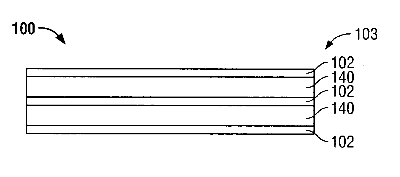
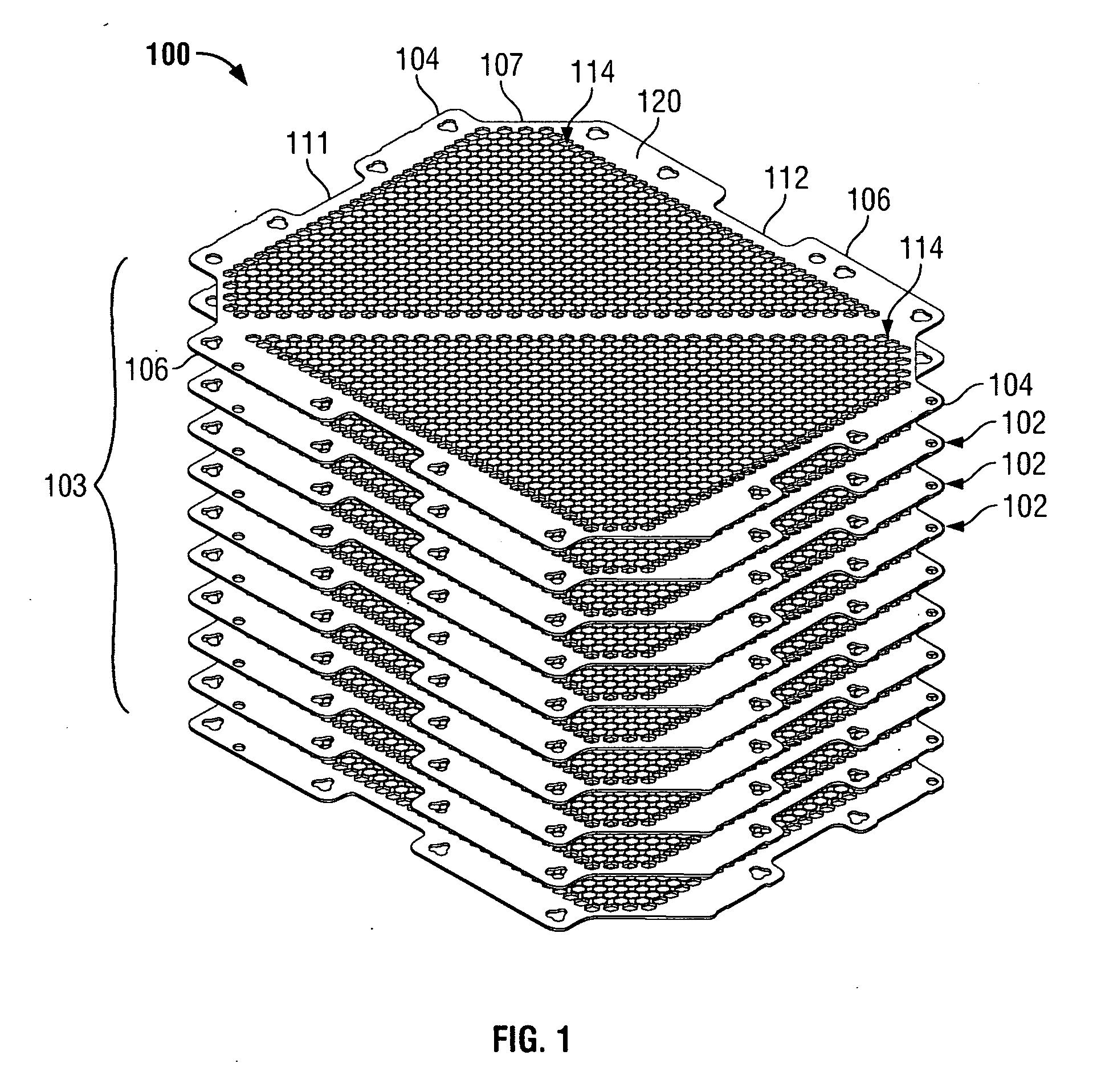
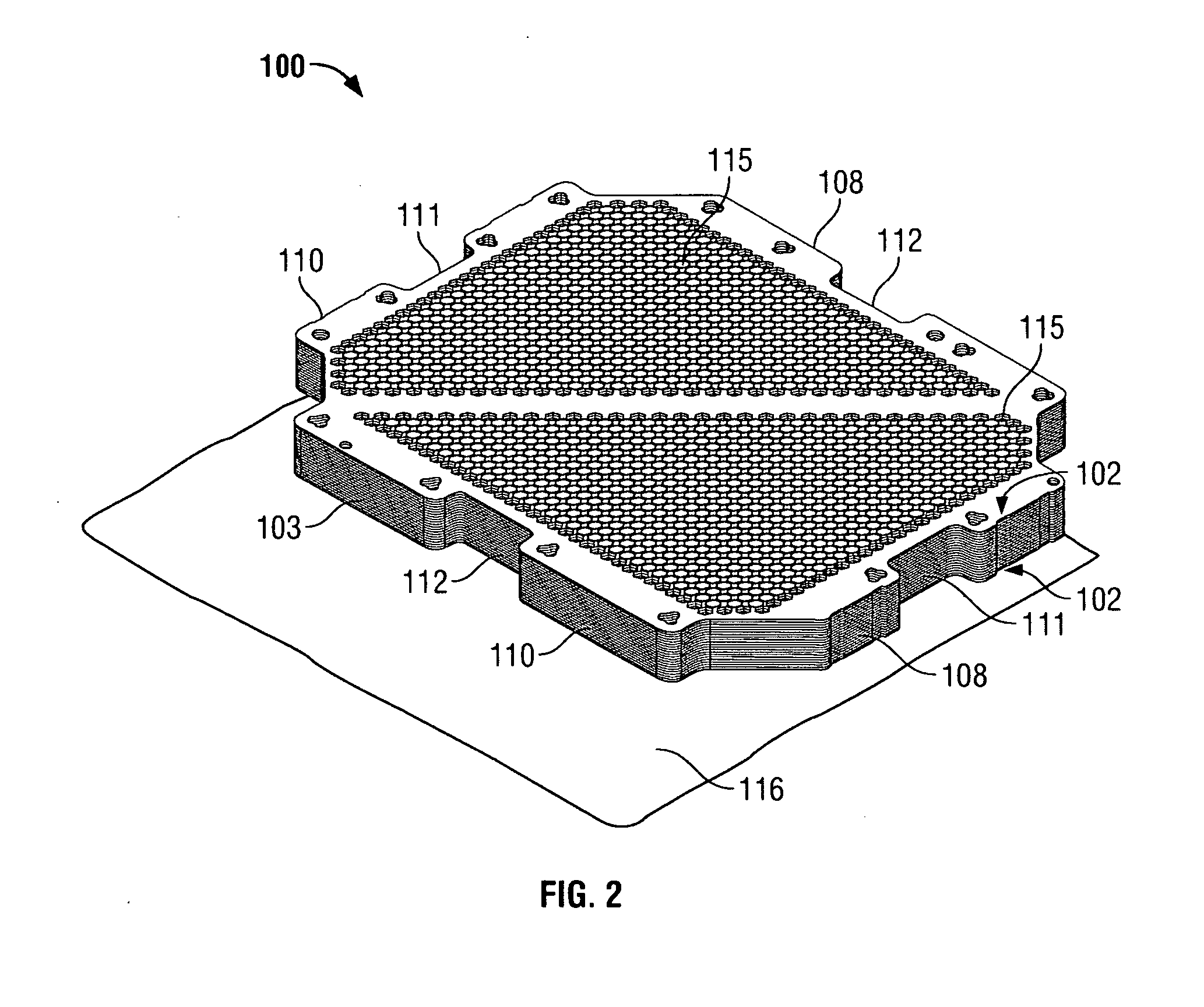
[0017]FIGS. 1 and 2 are an exploded perspective view and an assembled view, respectively, of an exemplary stacked metal laminate structure 100. As will become evident, below, the structure 100 is particularly advantageous for constructing a metal housing for an electrical connector, and more specifically to ball grid array (BGA) socket connector assembly which may be used to interface a ceramic microprocessor package with a circuit board. However, while the structure 100 is described in the context of a BGA socket connector, it is understood that the construction and methodology of the present invention as described hereinafter is not limited to housings for BGA socket assemblies, or even to electrical connectors for that matter. Rather, the illustrated embodiment is but one example of a conductive structure which may be formed in accordance with the inventive concepts herein.

[0018] In an exemplary embodiment, the structure 100 is fabricated from a plurality of separate or individu...


PUM

PropertyMeasurementUnit
thicknessaaaaaaaaaa
thicknessaaaaaaaaaa
thicknessaaaaaaaaaa

Abstract

A conductive structure and method of manufacturing therefor includes a plurality of stacked metal laminates secured to one another via an intermetallic bond made from a metallic bonding agent.

Description

BACKGROUND OF THE INVENTION [0001] This invention relates generally to three dimensional conductive structures and methods of making the same, and, more specifically, to the structure and manufacture of a metal laminated structure for a housing of an electrical connector. [0002] Due to advances in processor technology, signal transmission rates between electronic devices and components is increasing. With increased signal transmission rates, the need for effective shielding of signal contacts in electrical connectors interconnecting the electrical components is of greater importance. In at least some connectors, such as, for example, ball grid array (BGA) sockets which connect a microprocessor to a printed circuit board, metallized housings are advantageous. The metallized housing shields the signal contacts and prevents cross-talk, as well as provides a larger ground path than is typically available in non-conductive connectors. [0003] Conventionally, plastic housings have been man...

Claims


Application Information

Patent Timeline
Patent Type & Authority Applications(United States)
IPC IPC(8): H01R9/24H01R9/26H01R12/00H01R13/52H01R13/58H01R13/648H01R43/18
CPCH01R9/2416H01R9/2658H01R13/5205H01R13/582
Inventor HILTY, ROBERT DANIELMYERS, MARJORIE KAYLAUB, MICHAEL FREDRICK
Owner TE CONNECTIVITY CORP
Why Eureka
Try Eureka