High density nanostructured interconnection

a nano-structured, high-density technology, applied in the direction of vehicle sub-unit features, instrumentation, semiconductor/solid-state device details, etc., can solve the problems of increasing the risk of damage to the increasingly fragile components, damage to the mems package, damage to the mems components,

Active Publication Date: 2005-10-13
LUCENT TECH INC
View PDF8 Cites 39 Cited by
  • Summary
  • Abstract
  • Description
  • Claims
  • Application Information

AI Technical Summary

Benefits of technology

[0006] In another illustrative embodiment, a plurality of nanostructures is disposed on a component, such as a microprocessor, which is then brought into contact with a substrate. Intermolecular forces result in an attraction between the molecules of the nanostructures and the molecules of the substrate, thus creating a bond between the nanostructures and the substrate. In yet another illustrative embodiment, an intermediate layer having two nanostructured surfaces is disposed between a component and a substrate. The component and the substrate are each brought into contact with one of the nanostructured surfaces and a bond is created by intermolecular forces between the component and the intermediate layer as well as the substrate and the intermediate layer. Thus, a strong thermally and / or electrically conductive interconnection is created that is useful for applications in electronics packages without the temperature and force necessary in prior interconnection methods.

Problems solved by technology

However, while such gold-gold thermo-compression bonding is useful in many regards, the temperatures and pressures required to create such a bond may damage sensitive electronic elements, such as transistors.
As components become smaller and smaller, e.g., in MEMS devices, relatively high temperatures and pressures become more likely to cause damage to the increasingly fragile components.
However, once again, the temperature necessary to reflow the solder may damage MEMS components in the MEMS package.
Additionally, solder bumps have been limited by certain design considerations.
Additionally, since it is undesirable to have solder bumps come into contact with one another when the solder is reflowed, solder bumps must typically be separated by a minimum distance, for example, 50 microns from the center of one bump to the center of an adjacent bump.
However, such adhesives are typically subject to out-gassing as they cure which may introduce damaging organic material on critical electronics components that could interfere with proper performance of small components.

Method used


Image

  • High density nanostructured interconnection
  • High density nanostructured interconnection
  • High density nanostructured interconnection

Examples


Embodiment Construction

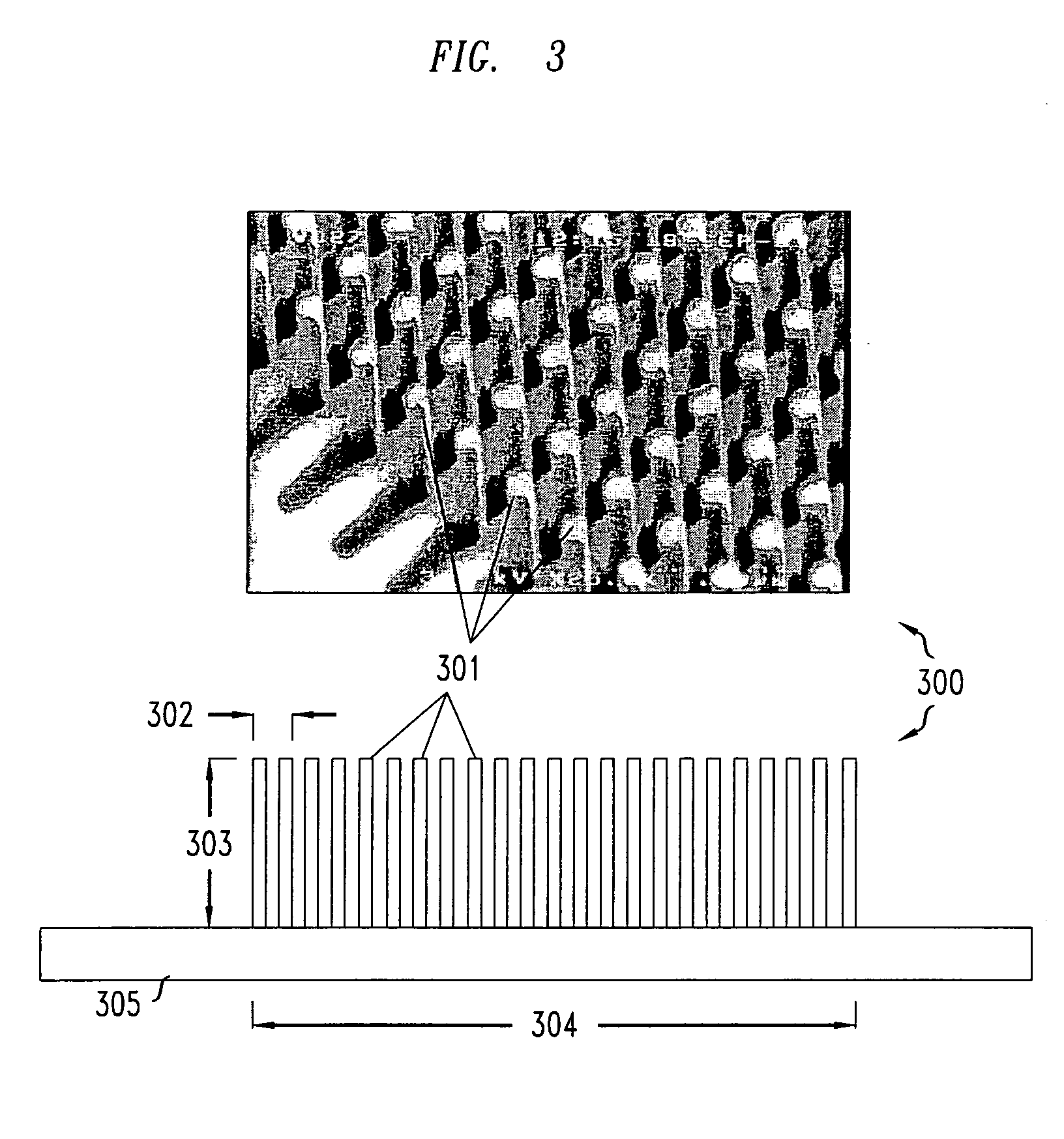
[0014]FIG. 3 shows one illustrative surface 300 in accordance with the principles of the present invention whereby a plurality of nanostructures 301, here nanoposts, are manufactured on a substrate 305, such as a silicon substrate. Cylindrical nanopost arrays, such as that shown in FIG. 3, have been produced with each nanopost having a diameter of less than 10 nm. One skilled in the art will recognize that there are many different illustrative arrangements (e.g., sizes, pitch and height) of nanoposts that can be produced using various methods and that such various diameter nanoposts can be fashioned with different degrees of regularity. An illustrative method of producing nanoposts, found in U.S. Pat. No. 6,185,961, titled “Nanopost arrays and process for making same,” issued Feb. 13, 2001 to Tonucci, et al, is hereby incorporated by reference herein in its entirety. Nanoposts have been manufactured by various methods, such as by using a template to form the posts, by various means ...


PUM


Abstract

A method and apparatus for forming an electrically and/or thermally conducting interconnection is disclosed wherein a first surface and a second surface are contacted with each other via a plurality of nanostructures disposed on at least one of the surfaces. In one embodiment, a first plurality of areas of nanostructures is disposed on a component in an electronics package such as, illustratively, a microprocessor. The first plurality of areas is then brought into contact with a corresponding second plurality of areas of nanostructures on a substrate, thus creating a strong friction bond. In another illustrative embodiment, a plurality of nanostructures is disposed on a component, such as a microprocessor, which is then brought into contact with a substrate. Intermolecular forces result in an attraction between the molecules of the nanostructures and the molecules of the substrate, thus creating a bond between the nanostructures and the substrate.

Description

FIELD OF THE INVENTION [0001] The present invention relates generally to thermal and electrical interconnections and, more particularly, to nanostructured thermal and electrical interconnections. BACKGROUND OF THE INVENTION [0002] Methods for electrically or thermally connecting electronics components onto, for example, a conductor or semiconductor substrate are well known in the art. For example, both thermo-compression and solder bump bonding methods have been used to create connections between, illustratively, components in optoelectronic devices and / or microelectromechanical (MEMS) devices. FIG. 1 shows one illustrative method of forming a thermo-compression bond for use as a thermal or electrical interconnection. Specifically, in that figure, component 101 has a layer of a material 102, typically gold, which is suitable for compression bonding. In order to bond component 101 with illustrative substrate 105, layer 102 on component 101 is, for example, lowered in direction 104 in...

Claims


Application Information

Patent Timeline
Patent Type & Authority Applications(United States)
IPC IPC(8): B82B1/00B81B7/00B82B3/00H01L21/60H01L21/768H01L23/373H01L23/485H01L23/49
CPCB81B7/0006B82Y10/00H01L24/12H01L24/16H01L24/90H01L2224/13099H01L2224/1319H01L2924/01013H01L2924/01015H01L2924/01022H01L2924/01027H01L2924/01033H01L2924/01079H01L2924/19043H01L2224/81345H01L2224/81385H01L2924/01006H01L2924/01019H01L2924/01055H01L2924/014H01L2224/13078H01L2924/1461H01L2924/00H01L2224/16105H01L2224/81193H01L2224/81194B60Q9/008B60Y2400/301B60Y2400/303B60Y2200/11
Inventor BASAVANHALLY, NAGESH R.CIRELLI, RAYMOND A.LOPEZ, OMAR DANIEL
Owner LUCENT TECH INC
Why Eureka
Try Eureka