Boost circuit and semiconductor integrated circuit

a technology of integrated circuits and boost circuits, applied in the field of boost circuits, can solve the problems of double power source voltage, increase the substrate area if used as well as the size of the chip, and high production cost, and achieve the effect of high voltage-boosting ratio

Active Publication Date: 2005-10-13
SEIKO EPSON CORP
View PDF6 Cites 12 Cited by
  • Summary
  • Abstract
  • Description
  • Claims
  • Application Information

AI Technical Summary

Benefits of technology

[0018] The present invention can provide the boost circuit with which a high voltage-boosting ratio can be obtained without using a large sized, high-voltage transistor, by including: the first boost means for generating the second power source potential having an absolute value larger than that of the first power source potential by conducting the charge pump operation using the clock signal whose high level or low level has been shifted; and the second boost means for generating the third power source potential having an absolute value larger than that of the second power source potential by conducting the charge pump operation using the clock signal whose high level and low level have been shifted.

Problems solved by technology

However, the high-voltage transistor is larger in size than the middle-voltage transistor, which increases the substrate area if used as well as the size of the chip and results in high production cost.
However, with this boost circuit, charging and discharging of the capacitor are carried out by use of two diodes, giving the boosted voltage of only about twice the power source voltage.

Method used


Image

  • Boost circuit and semiconductor integrated circuit
  • Boost circuit and semiconductor integrated circuit
  • Boost circuit and semiconductor integrated circuit

Examples


Embodiment Construction

[0026] In the following, a preferred embodiment to implement the present invention will be described in detail with reference to the accompanying drawings. Note that the same reference numbers are allotted to the same composition elements, and that descriptions thereof will be omitted.

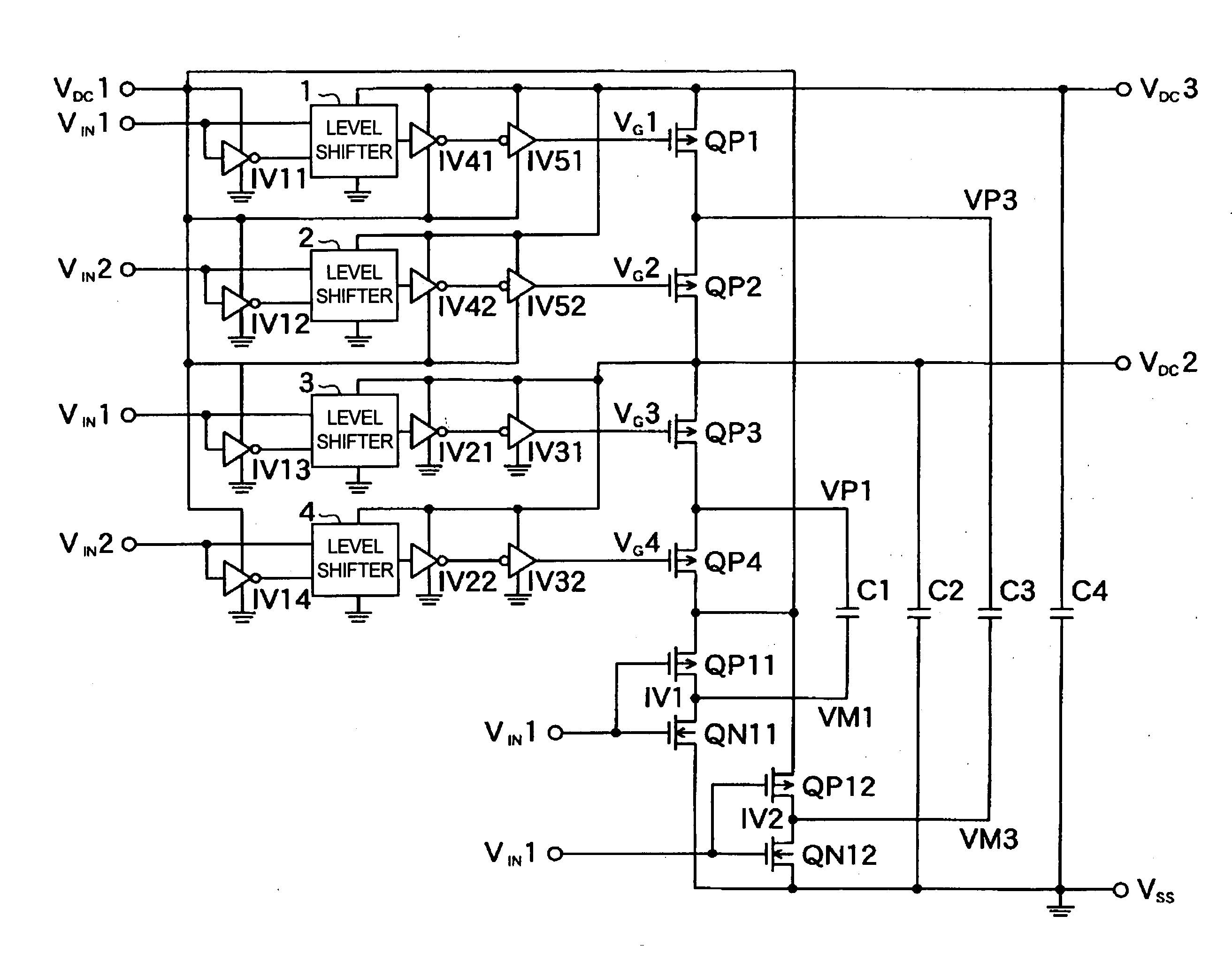
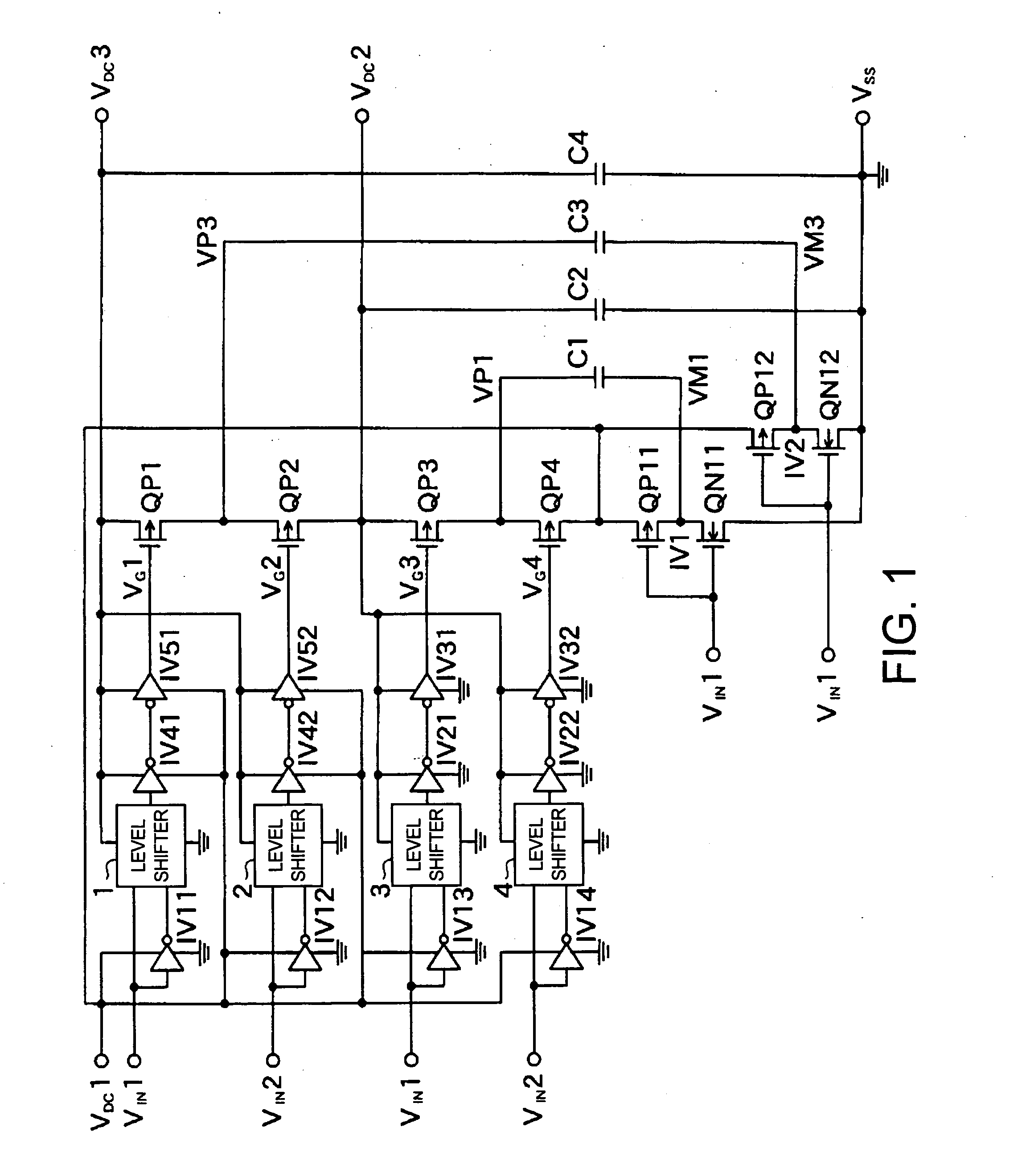
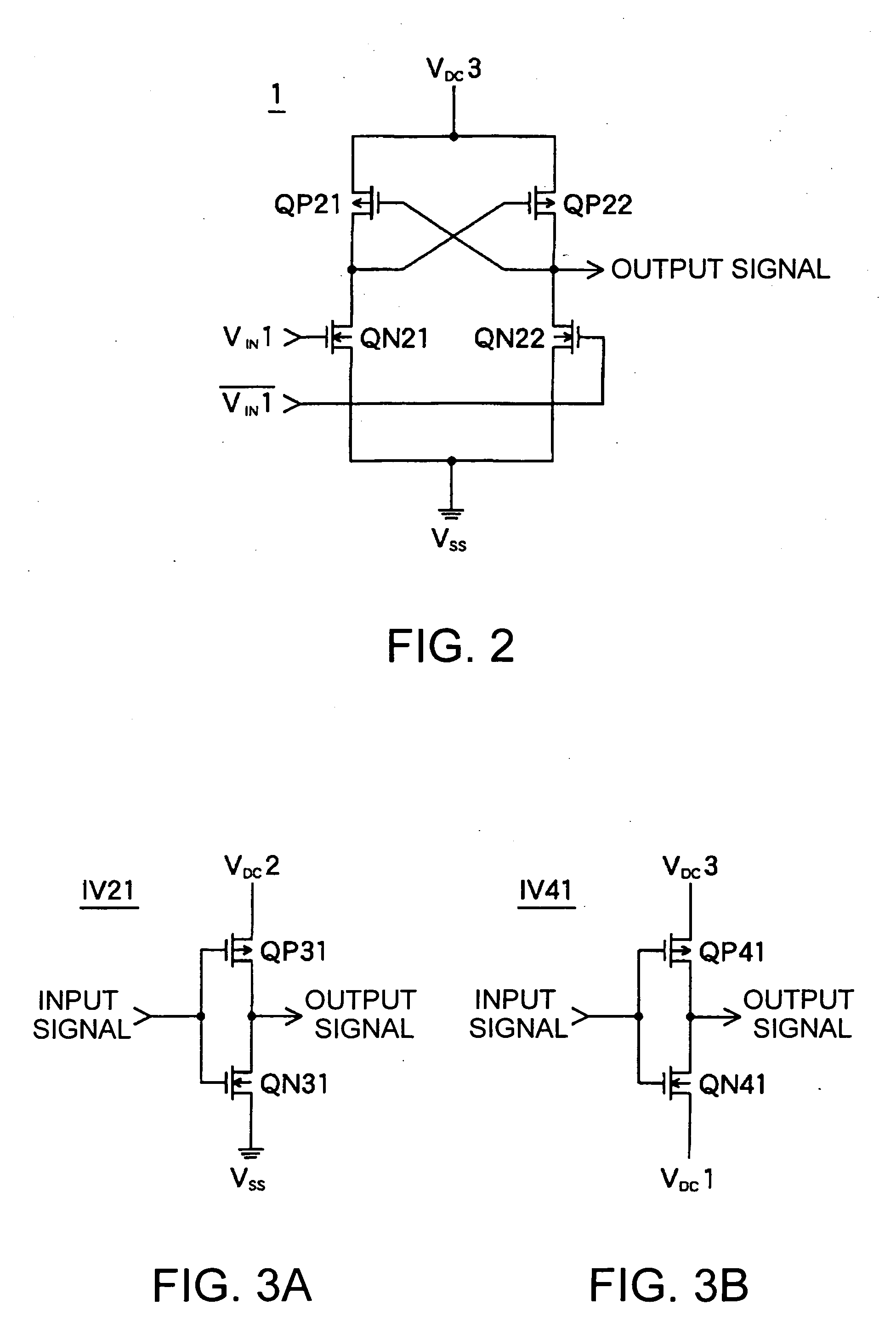
[0027]FIG. 1 is a diagram illustrating a configuration of the boost circuit according to one embodiment of the present invention. This boost circuit includes: P-channel MOS transistors QP1 to QP4 to carry out the charge pump operation, capacitors C1 to C4 coupled with these transistors, a P-channel MOS transistor QP11 and an N-channel MOS transistor QN11 composing a first inverter IV1, a P-channel MOS transistor QP12 and an N-channel MOS transistor QN12 composing a second inverter IV2, level shifters 1 to 4 and inverters IV11 to IV52 for supplying gate voltages VG1 to VG4 respectively to the transistors QP1 to QP4.

[0028] Here, the first boost means includes: the transistor QP4 having the source or th...


PUM


Abstract

A boost circuit includes: level shifters 3 and 4 for shifting a high level of a clock signal; a first boost means which contains transistors QP3 and QP4 for conducting switching in accordance with the clock signal whose high level has been shifted and capacitors C1 and C2 and, thereby, generates a power source potential VDC2 by conducting a charge pump operation; level shifters 1 and 2 for shifting a high level of a clock signal; inverters IV41 to IV52 for shifting a low level of the clock signal whose high level has been shifted; and a second boost means which contains transistors QP1 and QP2 for conducting the switching in accordance with the clock signal whose high level and low level have been shifted and capacitors C3 and C4 and, thereby, generates a power source potential VDC3 by conducting the charge pump operation.

Description

RELATED APPLICATIONS [0001] This application claims priority to Japanese Patent Application No. 2004-113774 filed Apr. 8, 2004 which is hereby expressly incorporated by reference herein in its entirety. BACKGROUND [0002] 1. Technical Field [0003] The present invention relates to a boost circuit utilizing a metal oxide semiconductor field effect transistor (MOS-FET). Further, the present invention relates to a semiconductor integrated circuit for realizing such a boost circuit. [0004] 2. Related Art [0005] For an example, it is known to use a boost circuit employing a charge pump method which utilizes the MOS-FET as a power source circuit of a thin-film transistor (TFT) driver IC for driving a liquid-crystal display. FIG. 6 shows a configuration of such a conventional boost circuit. This boost circuit includes: P-channel MOS transistors QP1 to QP3 that carry out the charge pump operation, capacitors C1 to C3 coupled with these transistors, a P-channel MOS transistor QP11 and an N-cha...

Claims


Application Information

Patent Timeline
Patent Type & Authority Applications(United States)
IPC IPC(8): H01L27/04G05F1/10H01L21/822H01L27/092H02M3/07
CPCH01L27/092H02M3/07
Inventor KOBAYASHI, HIRONORIYAMAGUCHI, HISASHI
Owner SEIKO EPSON CORP
Why Eureka
Try Eureka