Method of conductive particles dispersing

a technology of conductive particles and dispersible particles, which is applied in the direction of basic electric elements, electrical apparatus, and semiconductor devices, can solve the problems of reduced packaging process yield, reduced reliability of packaged ic, and high junction resistance of short circuit or high junction resistance, etc., and achieves low cost and simplified processes

Active Publication Date: 2005-10-13
IND TECH RES INST
View PDF10 Cites 21 Cited by
  • Summary
  • Abstract
  • Description
  • Claims
  • Application Information

AI Technical Summary

Benefits of technology

[0012] With the method for fixing the conductive particles according to the present invention, the conductive particles are positioned and fixed to the bumps of a chip precisely. The chip then can be bonded with a substrate using a non-conductive adhesive. The method according to the present invention is not only used in fine-pitch applications but also has advantages such as simplified processes and low costs. The conductive particles fixed by the present invention will not come off during subsequent processing. The present invention is therefore also applicable to the flip-chip packaging.

Problems solved by technology

However, when these methods are applied to the fine pitch bumping process, short circuit or high junction resistance due to solder joint bridging or missing phenomenon frequently happens.
It causes the reliability issues of the packaged IC devives, and reduce the yield of the packaging process.
The foregoing method taught by the U.S. Pat. No. 5,221,417 is more costly as additional ferromagnetic film and photo-lithography etching process are required.
However, the foregoing method is complicated, difficult to operate, and costly.
Moreover, as the diameter of the conductive particles is reduced, the pores of the screen have to be shrunk and the cost for producing the screen is increased as well.

Method used


Image

  • Method of conductive particles dispersing
  • Method of conductive particles dispersing
  • Method of conductive particles dispersing

Examples


Embodiment Construction

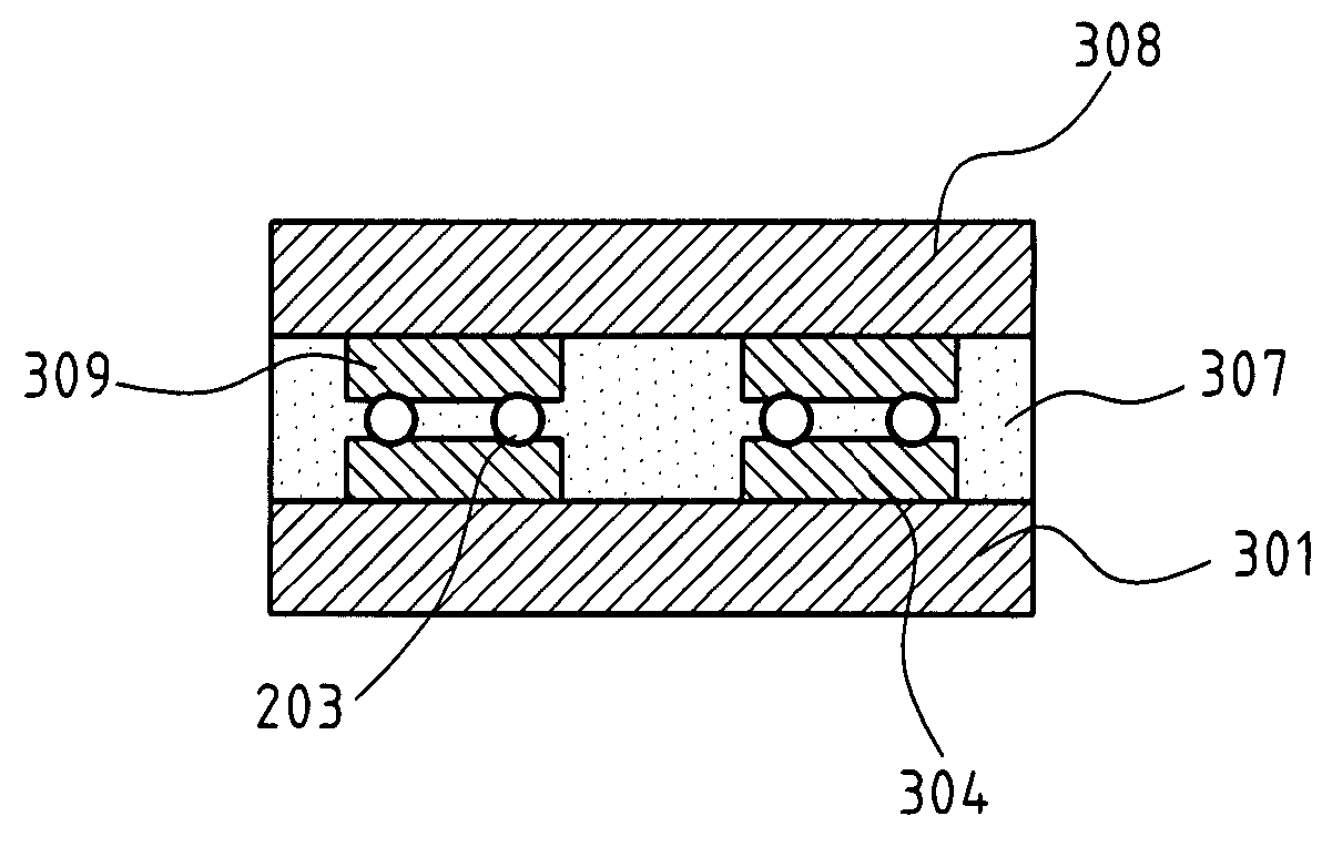
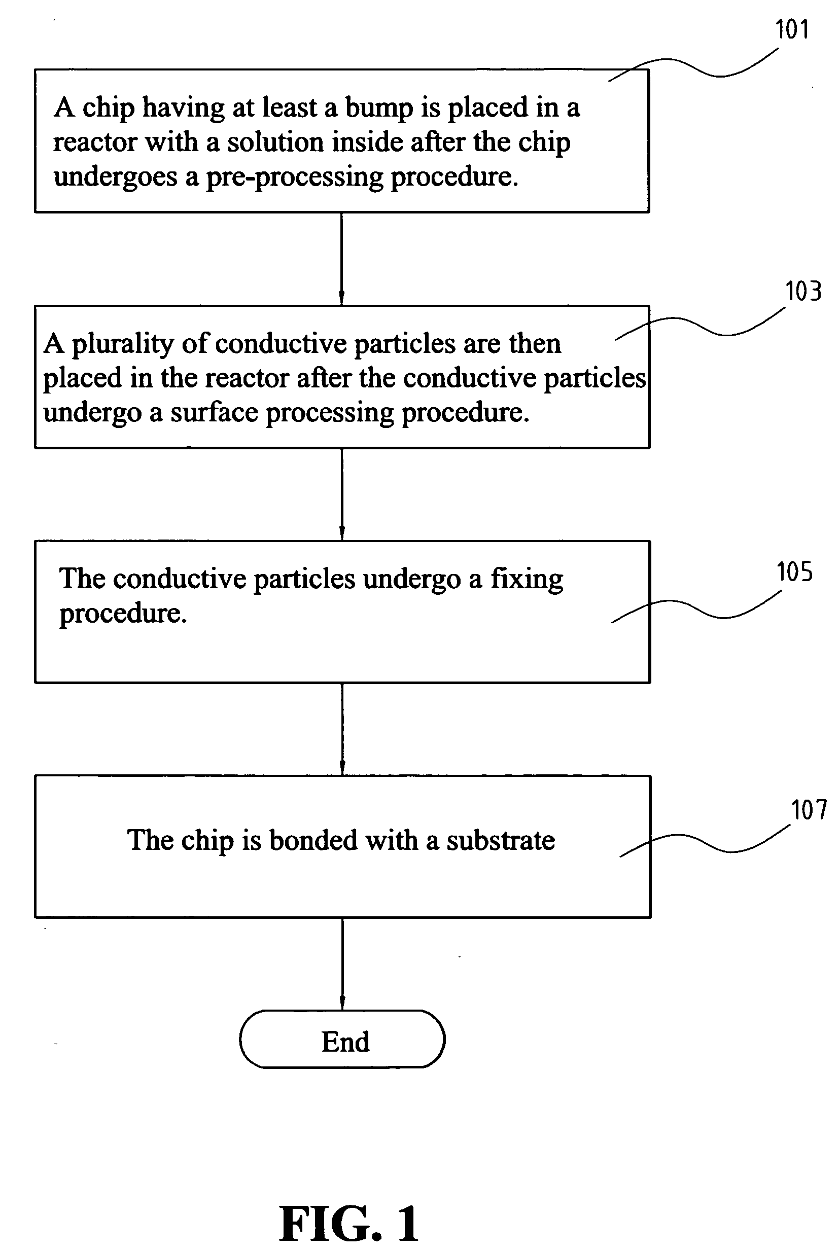
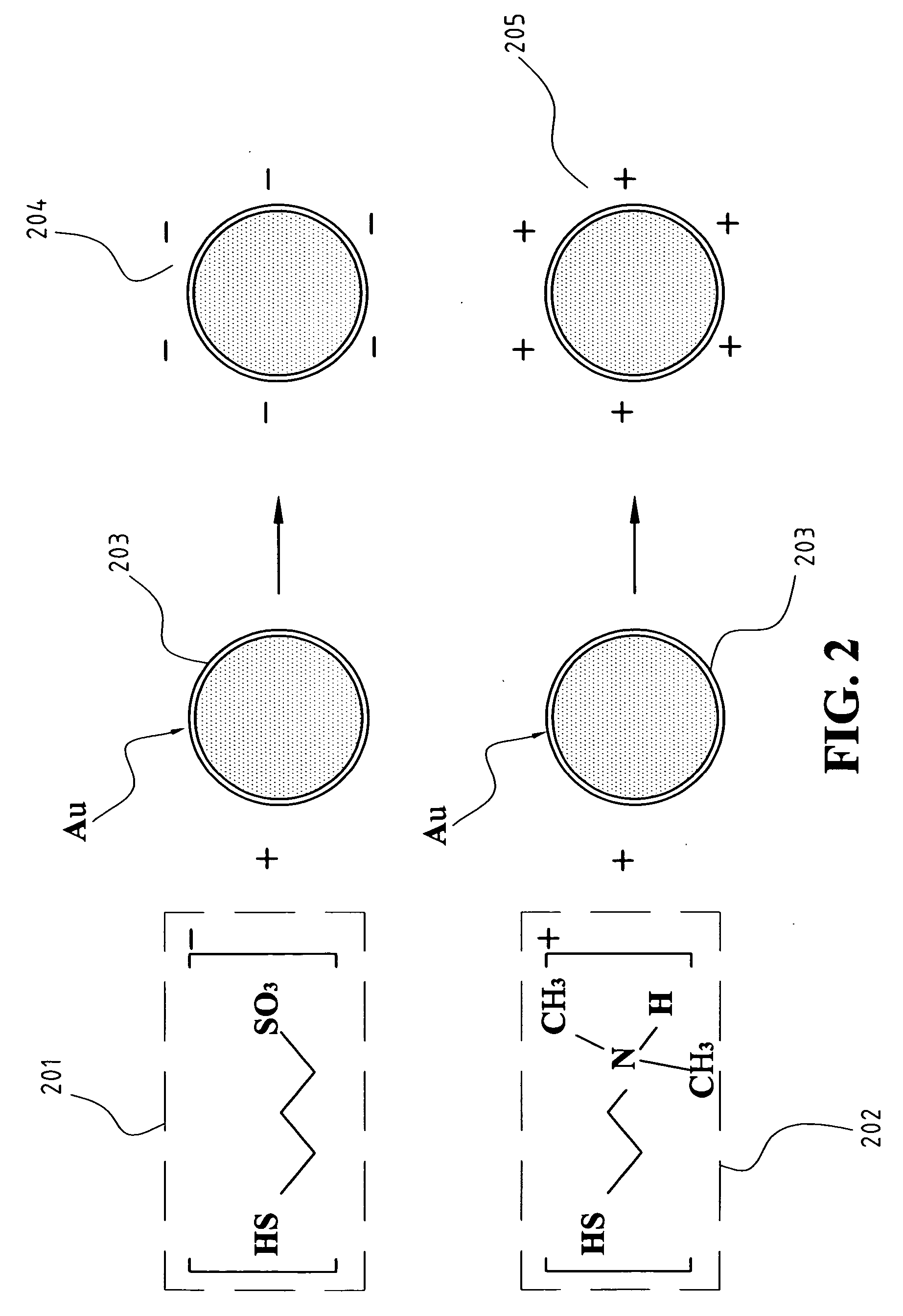
[0021]FIG. 1 is a flowchart showing the steps of the method for dispersing conductive particles according to the present invention. At the first step 101, a chip having at least a pad is placed in a reactor with a solution inside after the chip undergoes a pre-processing procedure. At the second step 103, a plurality of conductive particles are then placed in the reactor after the conductive particles undergo a surface processing procedure. The steps 101 and 103 can also be conducted in a reverse order. At the third step 105, the conductive particles undergo a fixing procedure. At last within the fourth step 107, the chip is bonded with a substrate. According to the present invention, within the pre-processing procedure of the first step 101, the chip is coated with a metallic layer and then an insulation layer, and the insulation layer on the bump is removed by etching. The surface processing procedure of the second step 103 causes the conductive particles to carry charges or carry...


PUM

PropertyMeasurementUnit
distanceaaaaaaaaaa
distanceaaaaaaaaaa
conductiveaaaaaaaaaa

Abstract

A method for dispersing conductive particles is provided, which takes advantages of simplified process and lower cost. The present invention is in applying of chemical bonding between metal and thiol with electric charge, thereby makes conductive particles and chip bumps carry charges. The conductive particles are then migrated and fixed to the bonding locations on the bumps of a chip through an electrophoresis procedure. The conductive particles will not come off during subsequent processes. The present invention can be applied to flip-chip packaging or other fine-pitch applications. With the present invention, the distance between bumps is smaller than 20 μm and the density of conductive particles is larger than 15 particles per bump.

Description

FIELD OF THE INVENTION [0001] The present invention generally relates to a method for dispersing conductive particles, and more specifically to a electrochemical method that allows conductive particles to be self-positioned and selectively dispersed on the electrodes of a chip or substrate. It is applicable to flip-chip packaging technologies. BACKGROUND OF THE INVENTION [0002] In semiconductor packaging technologies, flip-chip is the most promising type of packaging method. Related arts and patents have been constantly brought up to propose various improved methods. Among these flip-chip packaging methods, the methods using printing and metal jetting bumping process are the most competitive ones due to their lower costs. However, when these methods are applied to the fine pitch bumping process, short circuit or high junction resistance due to solder joint bridging or missing phenomenon frequently happens. It causes the reliability issues of the packaged IC devives, and reduce the y...

Claims


Application Information

Patent Timeline
Patent Type & Authority Applications(United States)
IPC IPC(8): H01L21/288H01L21/36H01L21/48H01L21/56H01L21/60
CPCH01L21/2885H01L21/4853H01L2924/07802H01L24/11H01L24/83H01L24/90H01L2224/13099H01L2224/838H01L2924/01029H01L2924/01079H01L2924/01082H01L2924/19042H01L2924/01005H01L2924/01006H01L2924/01033H01L2924/014H01L2924/00H01L2224/13078
Inventor CHEN, YU-CHIHUANG, RUOH-HUEYCHEN, YU-HUA
Owner IND TECH RES INST
Why Eureka
Try Eureka