Non-volatile storage device

a storage device and non-volatile technology, applied in the field of non-volatile storage devices, can solve the problems that the on-chip buffer unit cannot be effectively used practically during the erase operation, and cannot be carried out in such a manner

Inactive Publication Date: 2005-10-13
RENESAS ELECTRONICS CORP
View PDF8 Cites 50 Cited by
  • Summary
  • Abstract
  • Description
  • Claims
  • Application Information

AI Technical Summary

Benefits of technology

[0005] It is another object of the invention to provide a non-volatile storage device capable of quickly reading storage information read from the non-volatile memory unit and retained in the buffer unit to an outside independently of the operation of the non-volatile memory unit.

Problems solved by technology

First of all, the utilization of the buffer unit is not originally required in an erase operation for the non-volatile memory unit and cannot be applied to other uses.
For this reason, an on-chip buffer unit cannot be effectively used practically during the erase operation.
Moreover, the operation cannot be carried out in such a manner that storage information stored once in the buffer unit is to be read to an outside at a high speed independently of the operation of the non-volatile memory unit.

Method used


Image

  • Non-volatile storage device
  • Non-volatile storage device
  • Non-volatile storage device

Examples


Embodiment Construction

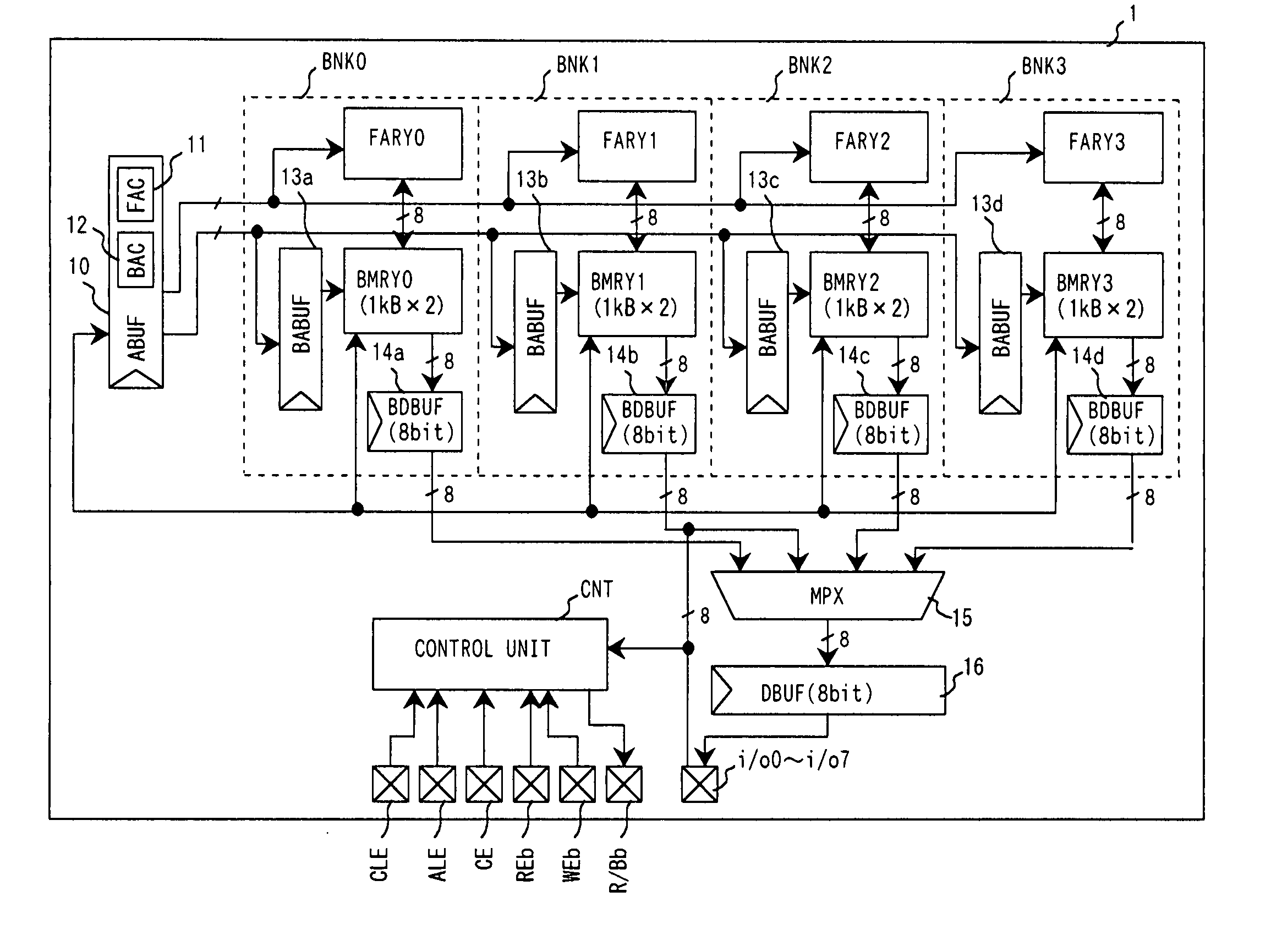
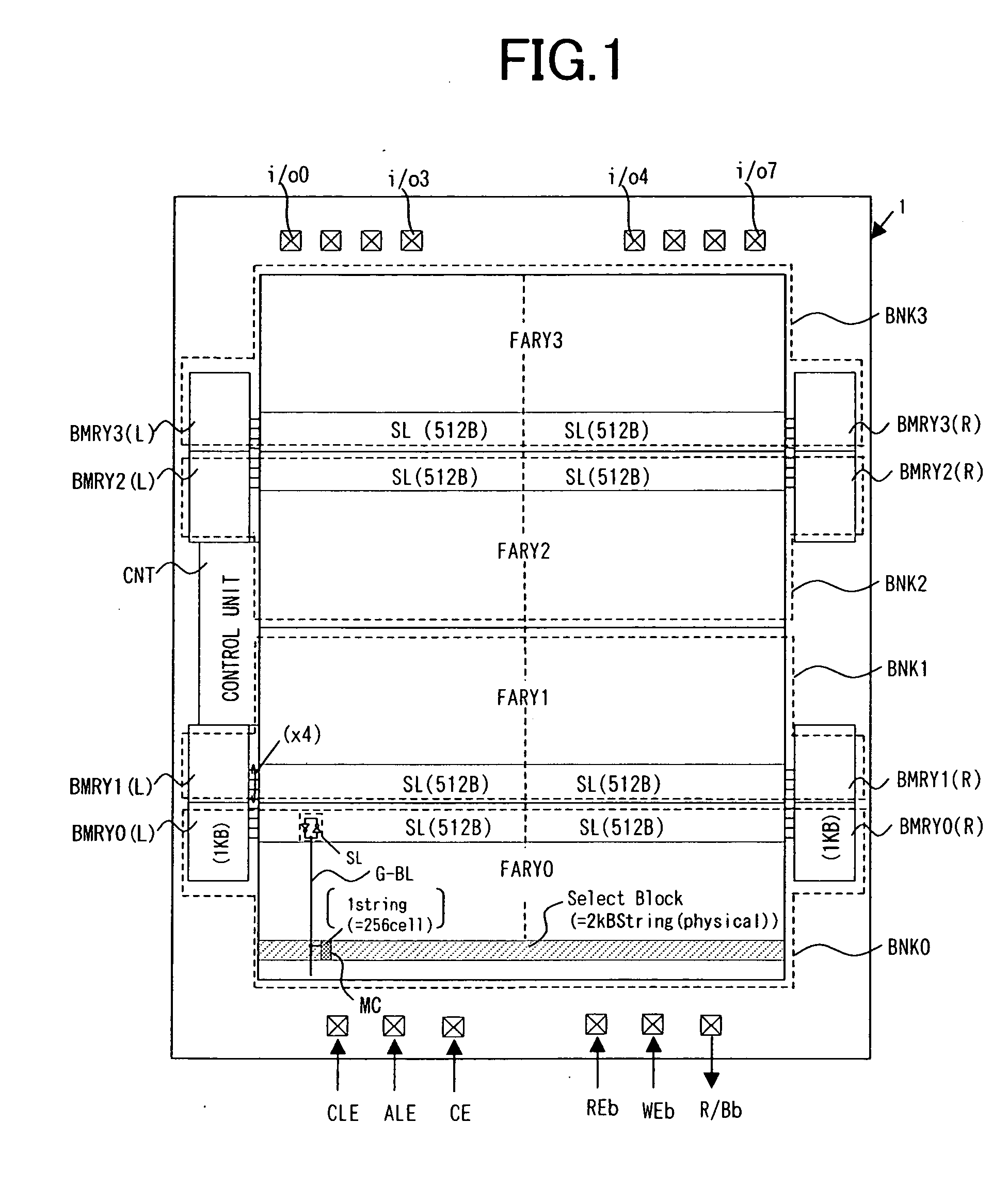
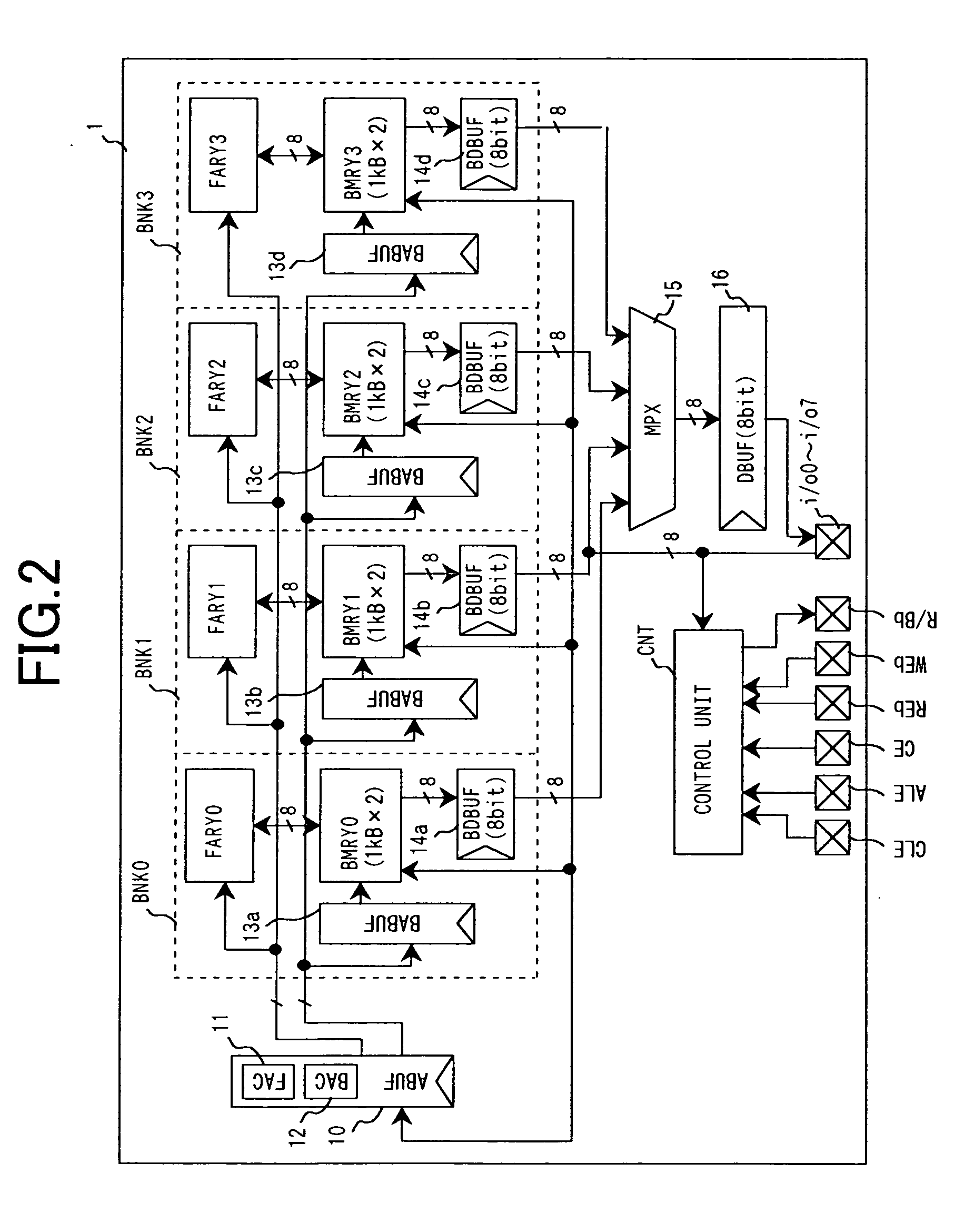
[0094]FIG. 1 shows the planar layout structure of a flash memory according to an example of a semiconductor storage device according to the invention. A flash memory 1 shown in FIG. 1 is not particularly restricted but is formed on one semiconductor substrate (chip) such as monocrystalline silicon by a well-known MOS integrated circuit manufacturing method.

[0095] The flash memory 1 has four memory banks BNK0 to BNK3 and a control unit CNT, for example. The memory banks BNK0 to BNK3 have flash memory arrays FARY0 to FARY3 to be non-volatile memory units and buffer memories BMRY0 to BMRY3 to be buffer units. The buffer memory is arranged with a transverse division into two parts corresponding to one flash memory array. For convenience, a suffix (R) is attached to the buffer memory on a right side and a suffix (L) is attached to the buffer memory on a left side.

[0096] External input / output terminals i / o0 to i / o7 of the flash memory 1 are also used as an address input terminal, a data...


PUM


Abstract

A non-volatile storage device (1) has non-volatile memory units (FARY0 to FARY3), buffer units (BMRY0 to BMRY3) and a control unit (CNT), and the control unit can control a first access processing between an outside and the buffer unit and a second access processing between the non-volatile memory unit and the buffer unit upon receipt of directives from the outside separately from each other. The control unit can independently carry out an access control over the non-volatile memory unit and the buffer unit in accordance with the directives sent from the outside, respectively. Therefore, it is possible to set up next write data to the buffer unit simultaneously with the erase operation of the non-volatile memory unit or to output once read storage information to the buffer unit at a high speed as in a cache memory operation in accordance with the directive sent from the outside. Consequently, it is possible to reduce the overhead of a data transfer for reading/writing data from/to the non-volatile storage device.

Description

CROSS-REFERENCE TO RELATED APPLICATION [0001] The present application claims priority from PCT international application PCT / JP02 / 11953 filed on Nov. 15, 2002, the content of which is hereby incorporated by reference into this application.BACKGROUND OF THE INVENTION [0002] The present invention relates to a non-volatile storage device having a non-volatile memory unit and a buffer unit thereof, and to an effective technology for an application to a flash memory having a multibank, for example. BACKGROUND ART [0003] JP-A-11-85609 has described a flash memory having a non-volatile memory unit and a buffer unit thereof. According to the publication, the memory unit can carry out read / write only on a unit of 8 bits or 16 bits, while it is necessary to exchange data on a unit of a single or plural sector(s) such as 512 bytes together with a host device, and therefore, the buffer unit is provided and utilized as a cache memory. The buffer unit to be utilized as the cache memory is simply ...

Claims


Application Information

Patent Timeline
Patent Type & Authority Applications(United States)
IPC IPC(8): G06F12/00G06F12/02G06F12/08G06F13/00G11C16/06G11C16/10G11C16/26
CPCG06F12/0246G06F12/0893G06F2212/2022G11C2216/22G11C16/06G11C16/10G11C16/26G06F2212/7203G06F12/00G11C16/00
Inventor TAKASE, YOSHINORIYOSHIDA, KEIICHIHORII, TAKASHINOZOE, ATSUSHITAMURA, TAKAYUKIFUJISAWA, TOMOYUKIMATSUBARA, KEN
Owner RENESAS ELECTRONICS CORP
Why Eureka
Try Eureka