Semiconductor integrated circuit equipment and its manufacture method

a technology of integrated circuit equipment and manufacturing method, which is applied in the direction of semiconductor devices, semiconductor/solid-state device details, electrical apparatus, etc., can solve the problems of more difficult to reduce the size of memory cells

Inactive Publication Date: 2005-10-20
RENESAS TECH CORP
View PDF10 Cites 7 Cited by
  • Summary
  • Abstract
  • Description
  • Claims
  • Application Information

AI Technical Summary

Benefits of technology

[0011] An object of the present invention is to provide a technique capable of suppressing the increase of the contact resistance at the interface between a metal layer and a silicon plug in the wiring structure in which the silicon plug is formed on and connected to the metal layer.
[0017] Since the trap layer is formed on the surface of the metal wiring in a region surrounding the silicon plug, the penetration of water into the interface between the plug and the metal wiring can be prevented in the thermal treatment performed in the manufacturing process. Consequently, since the high-resistance oxide layer is not formed at the interface between the silicon plug and the metal wiring, the increase of the contact resistance between the silicon plug and the metal wiring can be suppressed.

Problems solved by technology

Therefore, it is difficult to reduce the size of a memory cell.
Also, since the p type well region and the n type well region for forming the CMOS and the well isolation region for isolating the p type well region and the n type well region are required, it is more difficult to reduce the size of a memory cell.

Method used


Image

  • Semiconductor integrated circuit equipment and its manufacture method
  • Semiconductor integrated circuit equipment and its manufacture method
  • Semiconductor integrated circuit equipment and its manufacture method

Examples


Embodiment Construction

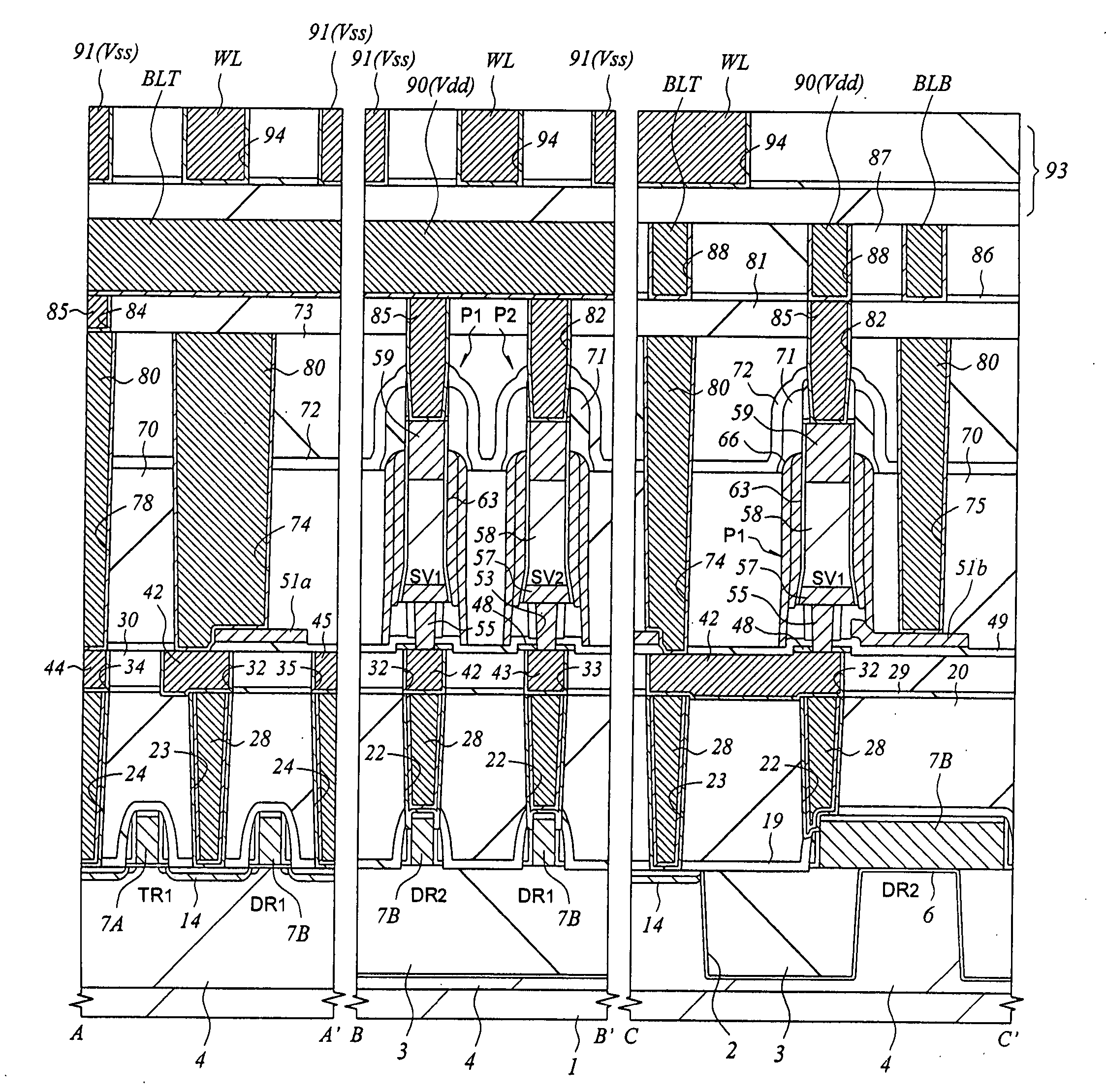
[0052] Hereinafter, embodiments of the present invention will be described in detail with reference to the accompanying drawings. Note that components having the same function are denoted by the same reference symbols throughout the drawings for describing the embodiment, and the repetitive description thereof will be omitted.

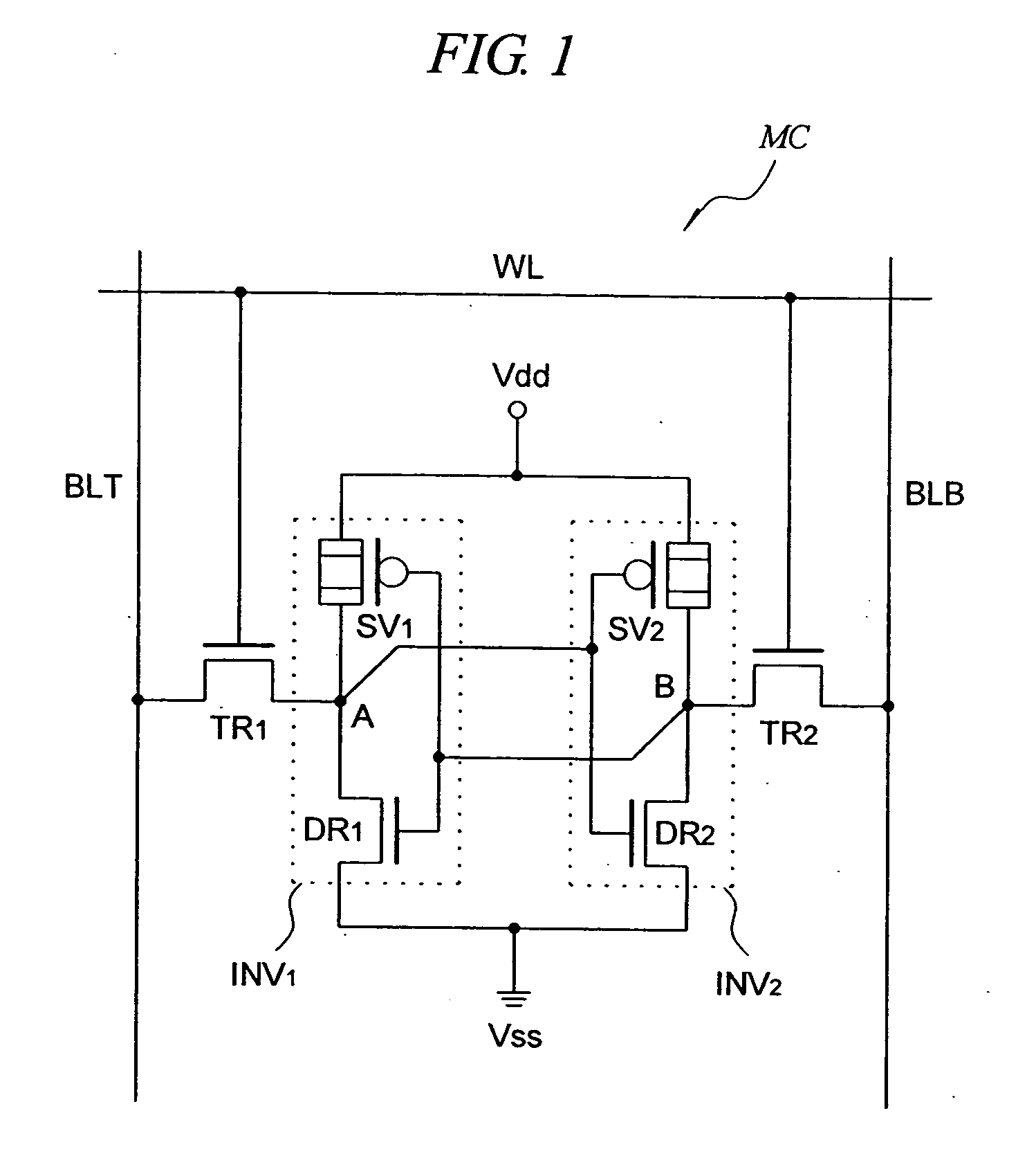
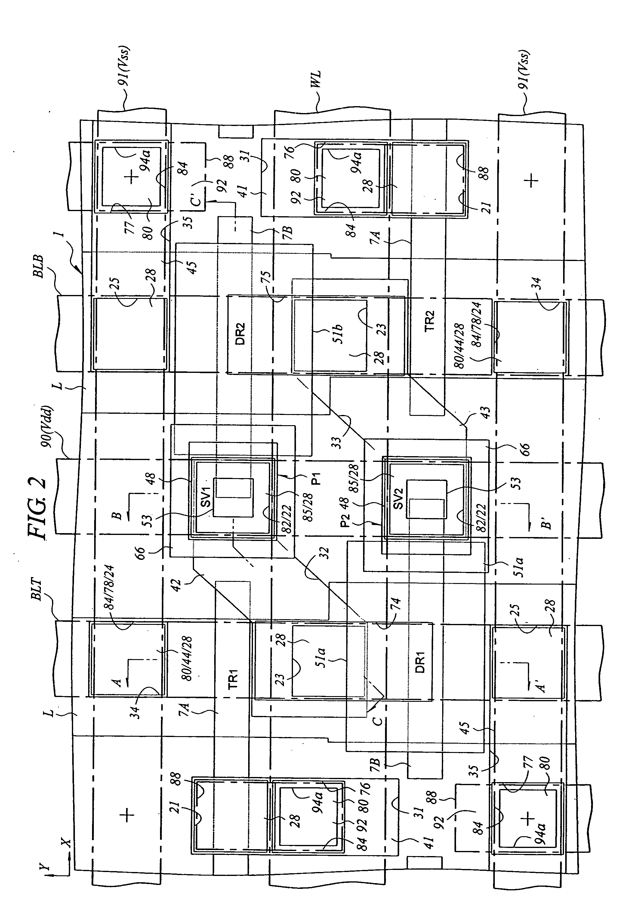
[0053]FIG. 1 is an equivalent circuit diagram of a memory cell of the SRAM according to an embodiment of the present invention. This memory cell MC of the SRAM is comprised of two transfer MISFETs (TR1, TR2), two driver MISFETs (DR1, DR2), and two vertical-type MISFETs (SV1, SV2) arranged at the intersection between a pair of complementary data lines (BLT, BLB) and a word line (WL).

[0054] Of the six MISFETs constituting the memory cell (MC), the two transfer MISFETs (TR1, TR2) and the two driver MISFETs (DR1, DR2) are composed of the n channel MISFETs, and the two vertical-type MISFETs (SV1, SV2) are composed of the p channel MISFETs. As described later, in t...


PUM

PropertyMeasurementUnit
power supply voltageaaaaaaaaaa
reference voltageaaaaaaaaaa
conductiveaaaaaaaaaa

Abstract

The object of the present invention is to suppress the increase of the contact resistance at the interface between the metal layer and the silicon plug in the wiring structure in which a metal layer is formed on and connected to a silicon plug. For its achievement, a lower semiconductor layer (drain) of a vertical-type MISFET is connected to an intermediate metal layer via an underlying plug composed of a polycrystalline silicon film, and a trap layer composed of a silicon nitride (TiN) film is formed on a part of the surface of the intermediate metal layer so as to surround the plug. The trap layer is formed in order to prevent an undesired high-resistance oxide layer from being formed at the interface between the plug and the intermediate metal layer.

Description

CROSS-REFERENCE TO RELATED APPLICATION [0001] The present application claims priority from Japanese Patent Application JP 2004-122428 filed on Apr. 19, 2004, the content of which is hereby incorporated by reference into this application. TECHNICAL FIELD OF THE INVENTION [0002] The present invention relates to a semiconductor integrated circuit device and manufacturing technology thereof. More particularly, the present invention relates to a technique effectively applied to a semiconductor integrated circuit device having wiring structure in which a silicon plug is laminated on a surface of metal wiring formed on a semiconductor substrate. BACKGROUND OF THE INVENTION [0003] In the SRAM (Static Random Access Memory) which is a type of a large-capacity semiconductor memory, a memory cell is comprised of four n channel MISFETs (Metal Insulator Field Effect Transistor) and two p channel MISFETs. [0004] However, in this type of SRAM, that is, in the so-called complete CMOS (Complementary ...

Claims


Application Information

Patent Timeline
Patent Type & Authority Applications(United States)
IPC IPC(8): H01L21/336H01L21/768H01L23/522H01L21/8234H01L21/8244H01L27/088H01L27/092H01L27/11H01L29/76
CPCH01L21/823425H01L21/823475H01L29/6656H01L27/092H01L27/11H01L27/088H10B10/00
Inventor MORIYA, SATOSHIKIKUCHI, TOSHIYUKIKONNO, AKIHIKOSATO, HIDENORIYAMAMOTO, NAOKIMATSUOKA, MASAMICHICHAKIHARA, HIRAKUNISHIDA, AKIO
Owner RENESAS TECH CORP
Why Eureka
Try Eureka