

Substrate processing apparatus
a processing apparatus and substrate technology, applied in the direction of manufacturing tools, liquid/solution decomposition chemical coating, electric circuit machining, etc., can solve the problems of reducing the reliability of plated films, reducing the reliability of copper interconnections, and increasing the problem of copper interconnection defects, etc., to achieve low cost and without lowering the throughput of apparatus
- Summary
- Abstract
- Description
- Claims
- Application Information
AI Technical Summary
Benefits of technology
Problems solved by technology
Method used
Image

Examples
first embodiment
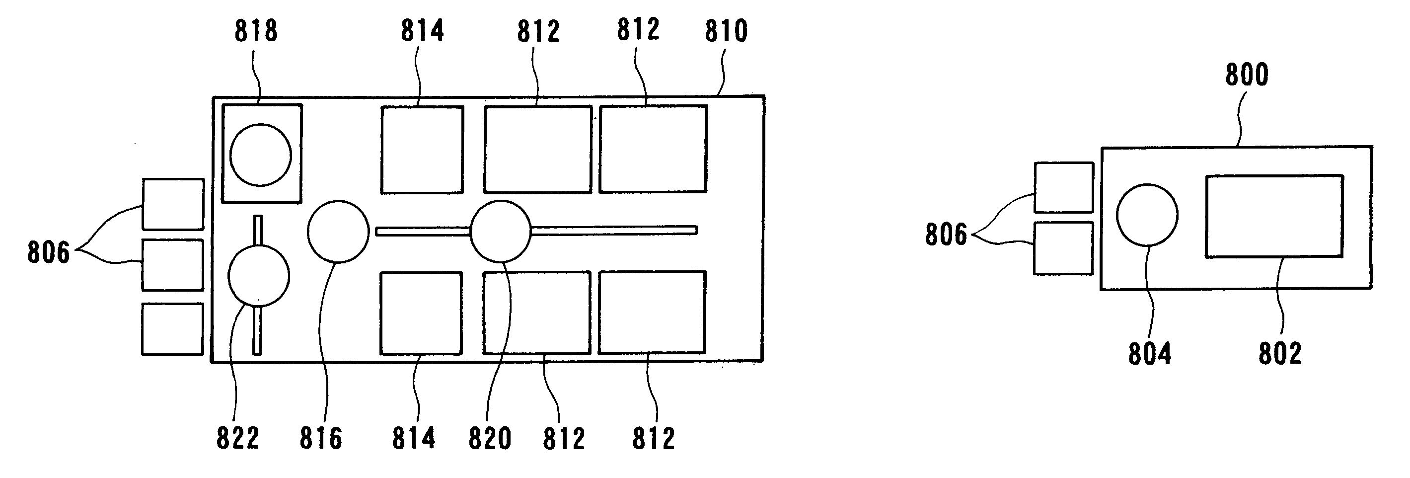
[0062]FIG. 5 is a plan view showing a substrate processing apparatus 1 according to the present invention. As shown in FIG. 5, the substrate processing apparatus 1 has a rectangular plating apparatus 2 for plating a substrate such as a semiconductor wafer having fine interconnection recesses and a rectangular additional process apparatus 3 for performing an additional process such as an annealing process, an etching process, or a polishing process on the substrate. The additional process apparatus 3 is connected to a longitudinal end of the plating apparatus 2. In the present embodiment, the plating apparatus 2 is employed as a main process apparatus for performing a main process on a substrate. However, the main process apparatus is not limited to a plating apparatus.
[0063] The plating apparatus 2 includes five plating units 20 each for plating a substrate to deposit metal on a surface of the substrate, two etching and cleaning units (cleaning and drying units) 22 each for etching,...
fourth embodiment
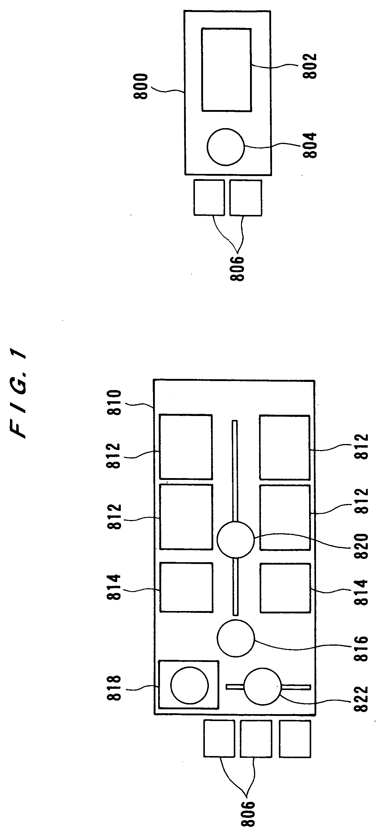
[0105]FIG. 13 is a plan view showing a substrate processing apparatus 301 according to the present invention. The substrate processing apparatus 301 has a rectangular plating apparatus 302 and two additional process apparatuses 303a and 303b. The plating apparatus 302 includes four plating units 20, two etching and cleaning units 22, a substrate placement stage 324 having a monitoring function, a substrate transfer device 28 movable along a longitudinal direction of the plating apparatus 302, a substrate transfer device 223 for transferring a substrate from or to substrate storage containers 4, a substrate placement stage 225 disposed between the substrate transfer device 28 and the substrate transfer device 223, a substrate placement stage 326a disposed adjacent to the additional process apparatus 303a, and a substrate placement stage 326b disposed adjacent to the additional process apparatus 303b. Each of the additional process apparatuses 303a and 303b has a substrate transfer de...
fifth embodiment
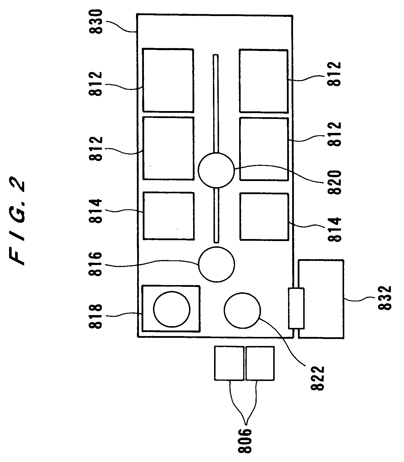
[0106]FIG. 14 is a plan view showing a substrate processing apparatus 401 according to the present invention. The substrate processing apparatus 401 has a rectangular plating apparatus 302 with a recess 402a and an additional process apparatus 403 disposed within the recess 402a. The plating apparatus 402 includes four plating units 20, two etching and cleaning units 22, a substrate placement stage 424 having a monitoring function, a substrate transfer device 28 movable along a longitudinal direction of the plating apparatus 402, a substrate transfer device 223 for transferring a substrate from or to substrate storage containers 4, and a substrate placement stage 225 disposed between the substrate transfer device 28 and the substrate transfer device 223. The substrate placement stage 225 is disposed adjacent to the additional process apparatus 403. The additional process apparatus 403 has a substrate transfer device 32 for transferring a substrate between the substrate placement sta...
PUM
| Property | Measurement | Unit |
|---|---|---|
| thickness | aaaaa | aaaaa |
| thickness | aaaaa | aaaaa |
| diameter | aaaaa | aaaaa |
Abstract
Description
Claims
Application Information