Direct-type backlight

Inactive Publication Date: 2005-10-27
NITTO DENKO CORP
View PDF2 Cites 25 Cited by
  • Summary
  • Abstract
  • Description
  • Claims
  • Application Information

AI Technical Summary

Benefits of technology

[0040] A shape and a size of the light reflecting section are not specifically limited as long as the function is shown and the advantage of the present invention is realized. However, the shape is preferably a circular shape and the size is preferably a size allowing the light reflecting section to be arranged further on an inner side than a groove closest to the center among the light scattering grooves.
[0041] It is possible to form the unevenness using a mold having unevenness of a pattern opposite to the unevenness of the light reflecting section on a surface thereof at the time of the resin sealing. For example, in the case of the transfer molding, the unevenness are formed by a transfer mold with the unevenness formed in a section corresponding to an upper surface of the resin sealing member. In the case of the casting, the unevenness are formed by pressing a surface of a resin layer formed by the casting using a press plate with the unevenness formed on a surface thereof. In the case of the laminate method, the unevenness are formed by pressing resin using a press plate with the unevenness formed on a surface thereof at the time of lamination.
[0042] As manufacturing of the mold, for example, a polyimide sheet is machined into a predetermined unevenness shape by laser machining and a nickel thin film is formed by electroless nickel plating to make a surface of the polyimide sheet smooth. Subsequently, the nickel thin film is transferred to the transfer mold and the press plate, whereby a mold for machining the unevenness in the light reflecting section is manufactured.
[0043] From the viewpoint of facilitating blocking and reflection of light directly emitted from the optical semiconductor element to the outside, it is preferable that a metal thin film is disposed on an upper surface of the light reflecting section. Examples of metal of the metal thin film include silver and aluminum. It is possible to form the metal thin film on the upper surface of the light reflecting section by, for example, masking and sputtering sections other than the light reflecting section. Note that, in the case of the resin sealing is performed by the transfer molding, since the unevenness are formed simultaneously with the molding, the formation of the metal thin film is performed after the formation of the unevenness. On the other hand, in the case of the resin sealing is performed by the casting or the laminate method, the formation of the metal thin film may be performed before or after the unevenness are formed by the press plate. A thickness of the metal thin film is preferably 0.05 to 0.5 μm.
[0044] In the present invention, the “light scattering grooves” refers to a section having a function of reflecting light emitted from the optical semiconductor element and scattering the light into the resin sealing member or on an upper surface of the resin sealing member.
[0045] In the present invention, plural light scattering grooves 5 are formed in a circular shape concentrically on at least one surface of at least one resin layer constituting the resin sealing member, and are arranged in such a manner that both of an area of a circle in the center and an area among the respective concentric circles are substantially the same. Here, the description “areas are substantially the same” means that the areas different from each other slightly are treated as “the same” areas as long as the advantage of the present invention is realized. For example, areas with a difference within a range of ±5% are treated as “areas that are substantially the same”. The difference is preferably within a range of +3%, more preferably within a range of +1%. Moreover, when the direct-type backlight of the present invention is viewed from a surface on which light emission is observed, the circular light scattering grooves 5 are preferably formed so as to surround the light reflecting section 4.

Problems solved by technology

However, in the planar light source device described above, sufficient uniformity of light emission in a plane has not been obtained yet.

Method used


Image

  • Direct-type backlight
  • Direct-type backlight
  • Direct-type backlight

Examples


manufacturing example 1

Mounting an Optical Semiconductor Element on a Wiring Circuit Board

[0052] A white board with a predetermined wiring pattern formed thereon (manufactured by Risho Kogyo Co., Ltd; CS-3965, length 30 mm×width 30 mm×thickness 600 μm) was prepared as a wiring circuit board and an optical semiconductor element (manufactured by Showa Denko K. K.; SOA-230U) was mounted on the white board by wire bonding to prepare a wiring circuit board with the optical semiconductor element mounted thereon.

manufacturing example 2

Manufacturing Press Plate A

[0053] A light reflecting section and light scattering grooves having shapes shown below were formed on a polyimide sheet by laser machining, and a nickel thin film was formed by nickel plating to make a machined surface thereof smooth. Press plate A was prepared by transferring the obtained nickel thin film.

Shape of the Light Reflecting Section

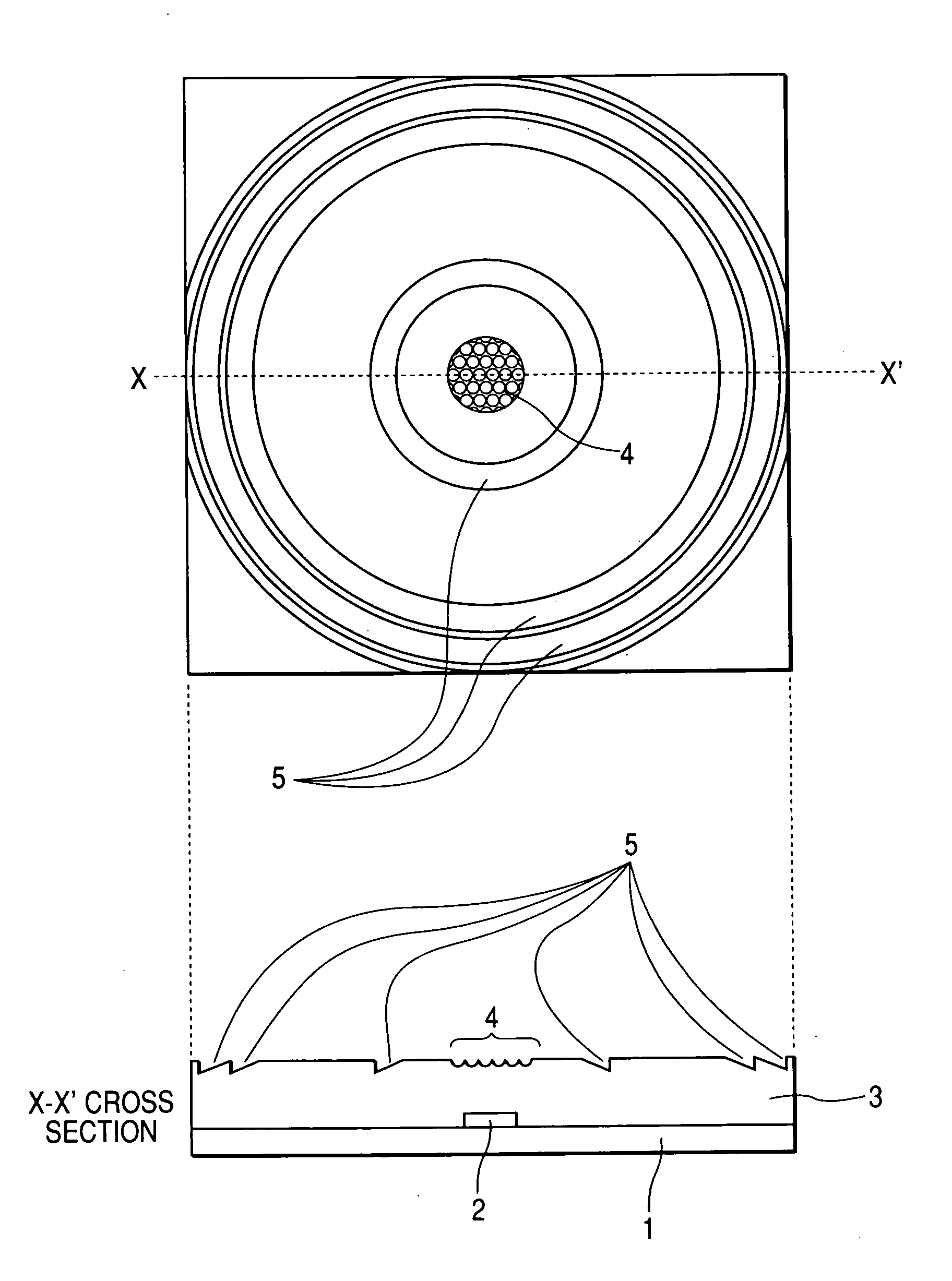
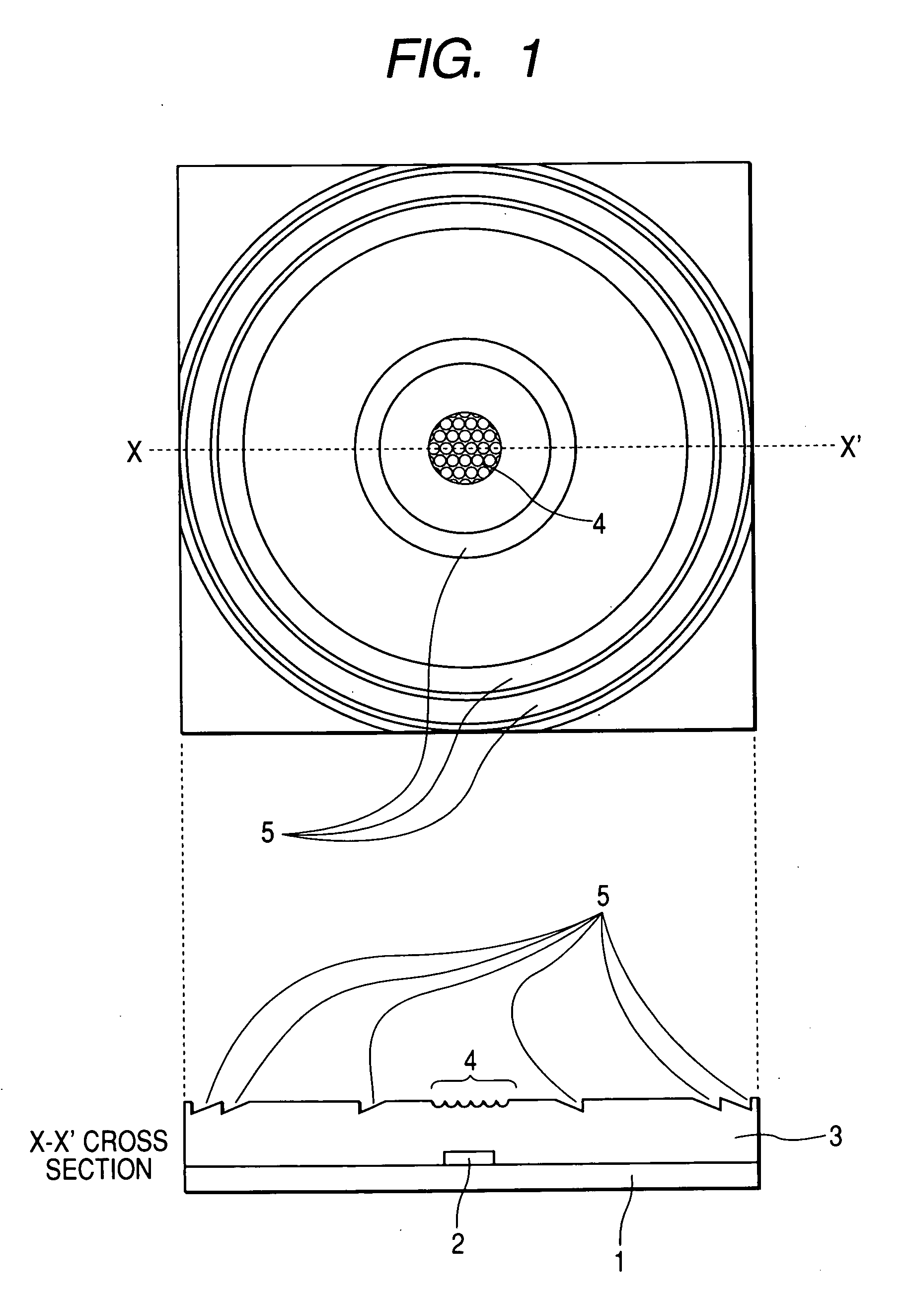
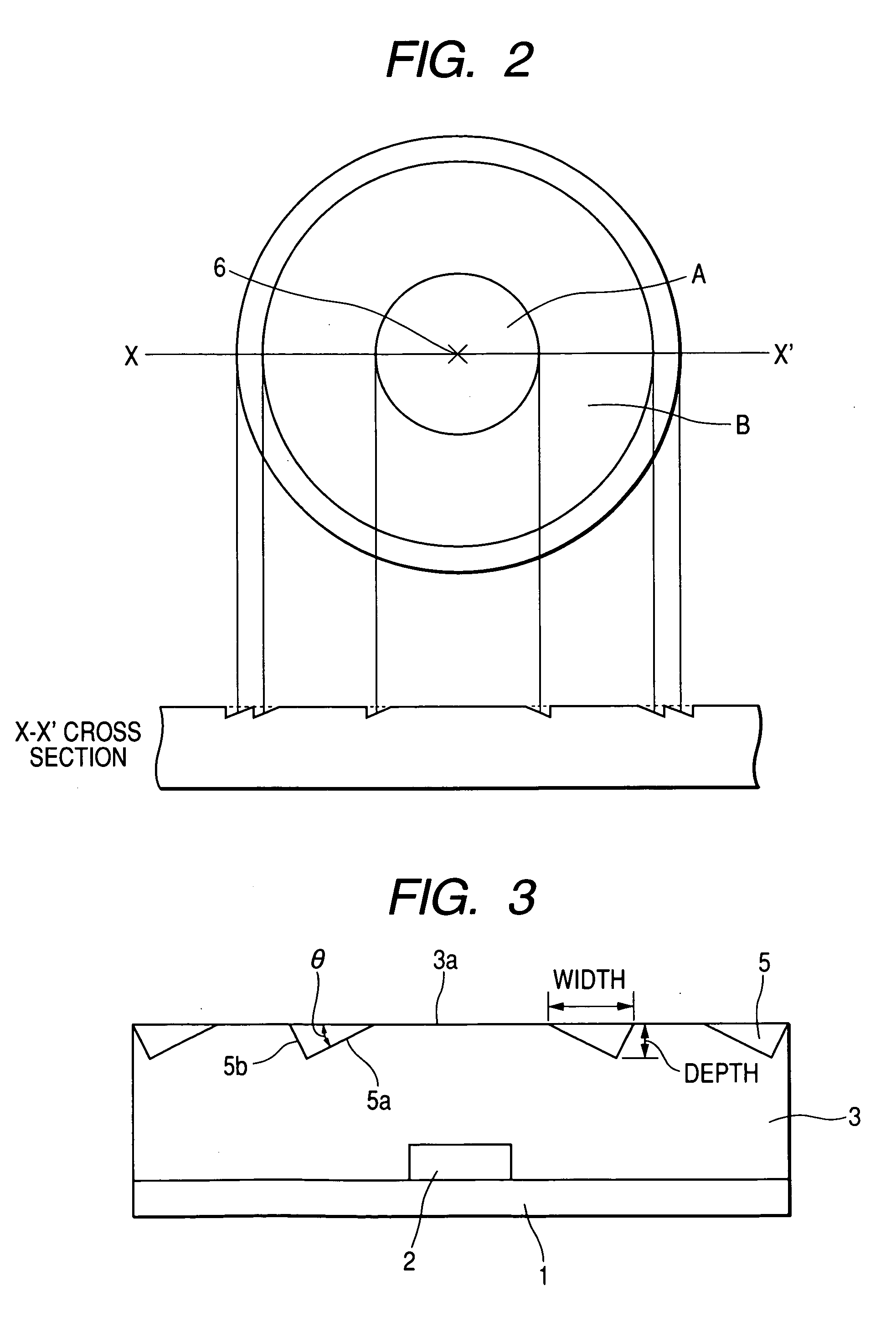
[0054] An unevenness of a semispherical shape with a radius of 20 μm, a height of 25 μm, and a pitch of 60 μm in a circle having a radius of 1 mm with a position corresponding to a center of gravity of an optical semiconductor element as a center

Shape of the Light Scattering Grooves

[0055] An area of a circle in the center: 7.1 mm2 (radius of about 1.5 mm)

[0056] The number of concentric circles: 200

[0057] An area among respective concentric circles: 7.1 mm2 (a radius of an outermost circle of about 21.2 mm)

[0058] A shape of grooves: width of 30 μm, depth of 17 μm, a sectional shape of a right triangle (θ1 of ...

manufacturing example 3

Manufacturing Press Plate B

[0059] A light reflecting section having a shape shown below was formed on a polyimide sheet by laser machining and a nickel thin film was formed by nickel plating to make a machined surface thereof smooth. Press plate B was manufactured by transferring the obtained nickel thin film.

Shape of the Light Reflecting Section

[0060] An unevenness of a semispherical shape with a radius of 20 μm, a height of 25 μm, and a pitch of 60 μm in a circle having a radius of 1 mm with a position corresponding to a center of gravity of an optical semiconductor element as a center


PUM


Abstract

The present invention provides A direct-type backlight having: a resin sealing member including at least one resin layer, which has a light reflecting section formed on the outermost surface of the resin sealing member; an optical semiconductor element sealed by the resin sealing member; and plural circular light scattering grooves formed concentrically on at least one surface of the resin layer, wherein an area of a circle in the center and an area among the respective concentric circles are substantially the same.

Description

FIELD OF THE INVENTION [0001] The present invention relates to a direct-type backlight that is used in a liquid crystal display. BACKGROUND OF THE INVENTION [0002] A planar light source device using an optical semiconductor element (an LED), in which a large number of grooves having a shape of a semicircular on cross section are formed concentrically in order to scatter light, is reported (see, for example, reference 1). [0003] [Reference 1] JP 2000-184137 A [0004] However, in the planar light source device described above, sufficient uniformity of light emission in a plane has not been obtained yet. [0005] It is an object of the present invention to provide a direct-type backlight that has a more uniform amount of light emission in a plane. SUMMARY OF THE INVENTION [0006] The present inventors have made eager investigation to examine the problem. As a result, it has been found that the foregoing objects can be achieved by the following direct-type backlight and lighting device. Wit...

Claims


Application Information

Patent Timeline
IPC IPC(8): G02F1/1335F21S2/00F21V5/00F21Y101/02G02F1/13357H01L33/00H01L33/54H01L33/56
CPCG02F1/133603Y10S362/80H01L2933/0091H01L33/54
Inventor SUEHIRO, ICHIROHOTTA, YUJISADAYORI, NAOKIHARADA, NORIAKIUAWADA, KAZUKI
Owner NITTO DENKO CORP
Why Eureka
Try Eureka