Method for growth of group III-V semiconductor material on a dielectric
- Summary
- Abstract
- Description
- Claims
- Application Information
AI Technical Summary
Benefits of technology
Problems solved by technology
Method used
Image
Examples
Embodiment Construction
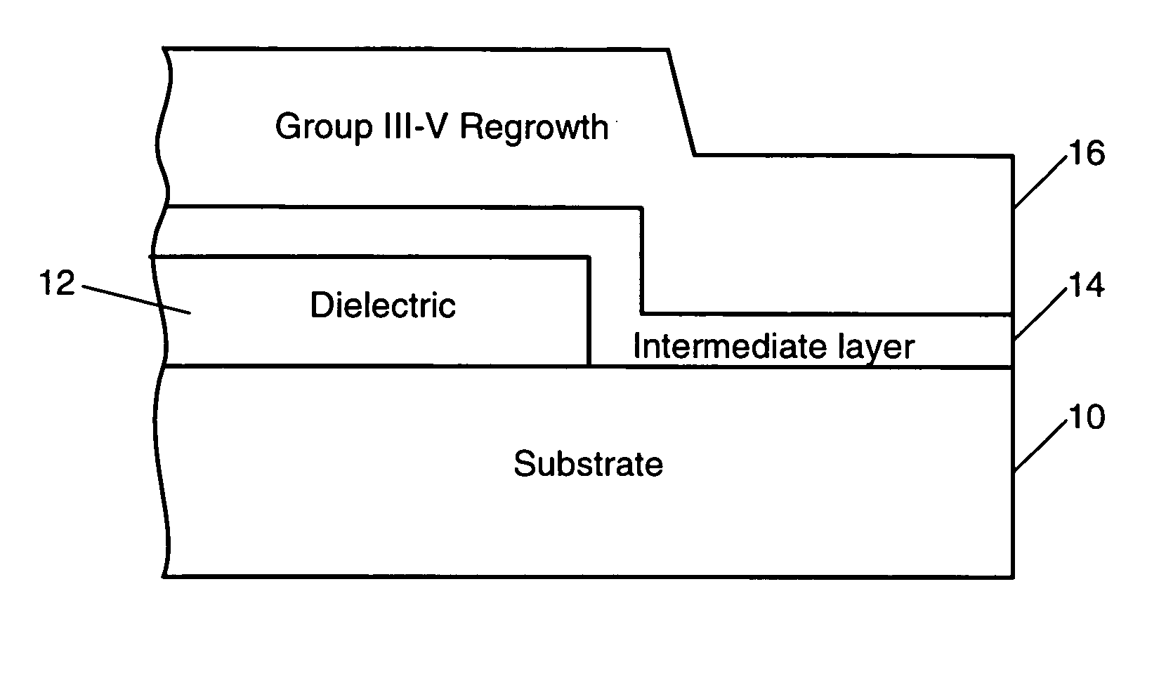
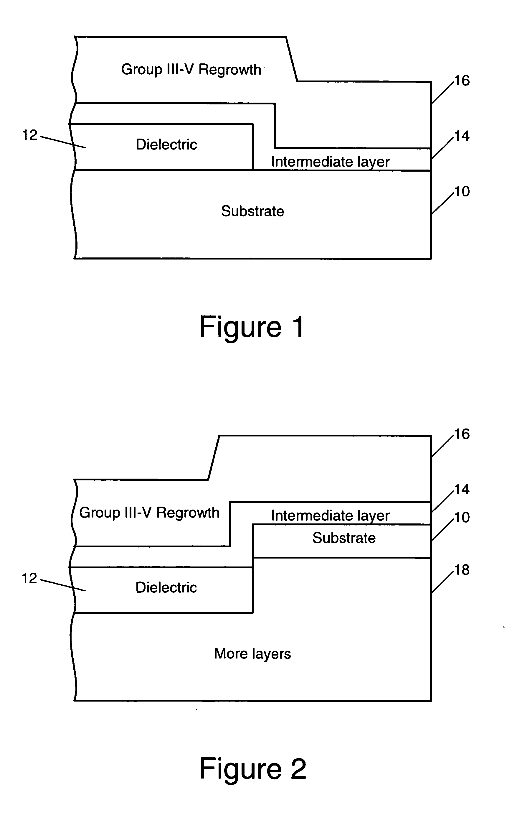
[0010] As shown in the drawing for purposes of illustration, the present invention is concerned with semiconductor fabrications techniques and, in particular, with a fabrication method that facilitates the use of Group III-V semiconductor materials in structures that include dielectric layers. Group III-V materials have important applications in high-speed semiconductor structures, such as heterojunction bipolar transistors (HBTs), high electron mobility transistors (HEMTs), and various electro-optical devices. As discussed above, Group III-V semiconductor materials in general have undesirable electrical and morphology properties that render them difficult to work with in structures that include dielectric layers.
[0011] In accordance with the present invention, before a Group III-V material is regrown over a semiconductor structure, an intermediate layer, or seed layer, is first grown. The intermediate layer is selected to have a relatively smooth morphology, which results in impro...
PUM
 Abstract
Description
Claims
Application Information

