Method for dicing wafer and process for manufacturing liquid-discharging head using the dicing method

Inactive Publication Date: 2005-11-03
CANON KK
View PDF11 Cites 10 Cited by
  • Summary
  • Abstract
  • Description
  • Claims
  • Application Information

AI Technical Summary

Benefits of technology

[0017] The present invention is directed to a method for dicing a wafer having openings arranged in a face thereof and a process for manufacturing a liquid-discharging head using the dicing method. The dicing method prevents adhesive cutting dust from remaining in the openings when the wafer is diced.
[0019] In one aspect of the present invention, a method for dicing a wafer having a first face, dicing streets, and opening arranged along the dicing streets, is provided. This dicing method includes a step of affixing a dicing tape having adhesive regions to the first face such that the dicing tape lies over the openings and the adhesive regions are exposed in the openings, and a step of treating the dicing tape to reduce an adhesive strength of the adhesive regions.

Problems solved by technology

However, this technique has a problem in that alignment must be performed before the protective tape is affixed to the wafer, increasing the number of manufacturing steps.

Method used


Image

  • Method for dicing wafer and process for manufacturing liquid-discharging head using the dicing method
  • Method for dicing wafer and process for manufacturing liquid-discharging head using the dicing method
  • Method for dicing wafer and process for manufacturing liquid-discharging head using the dicing method

Examples


first embodiment

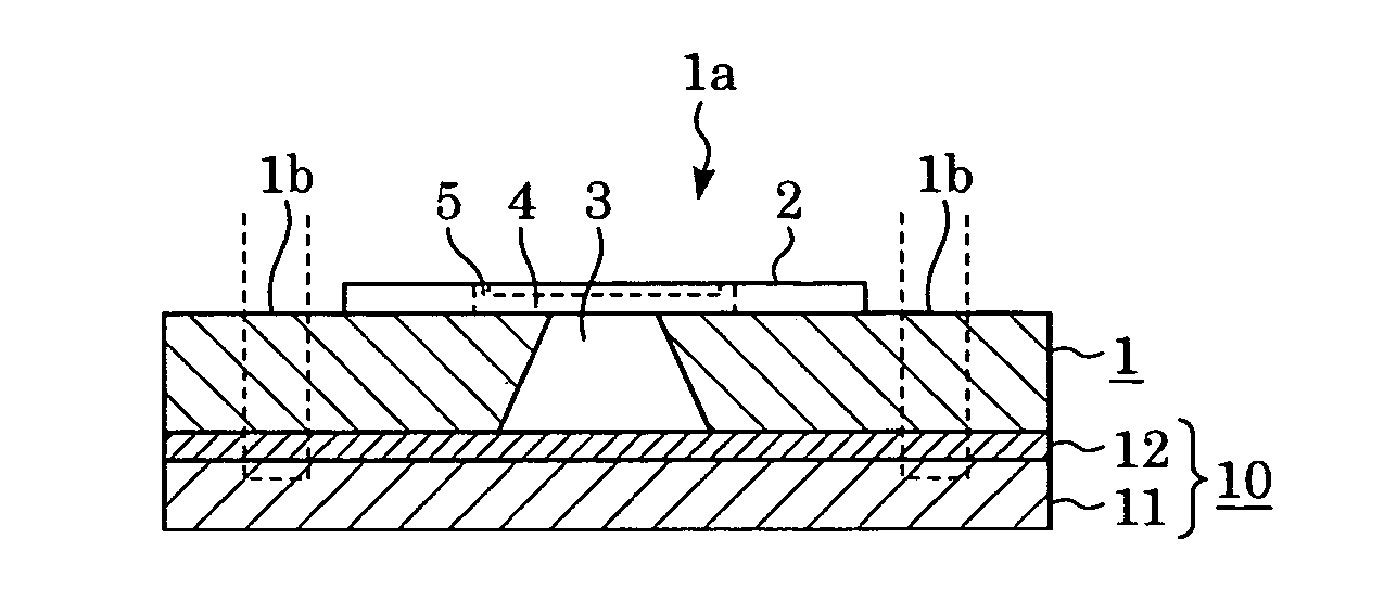
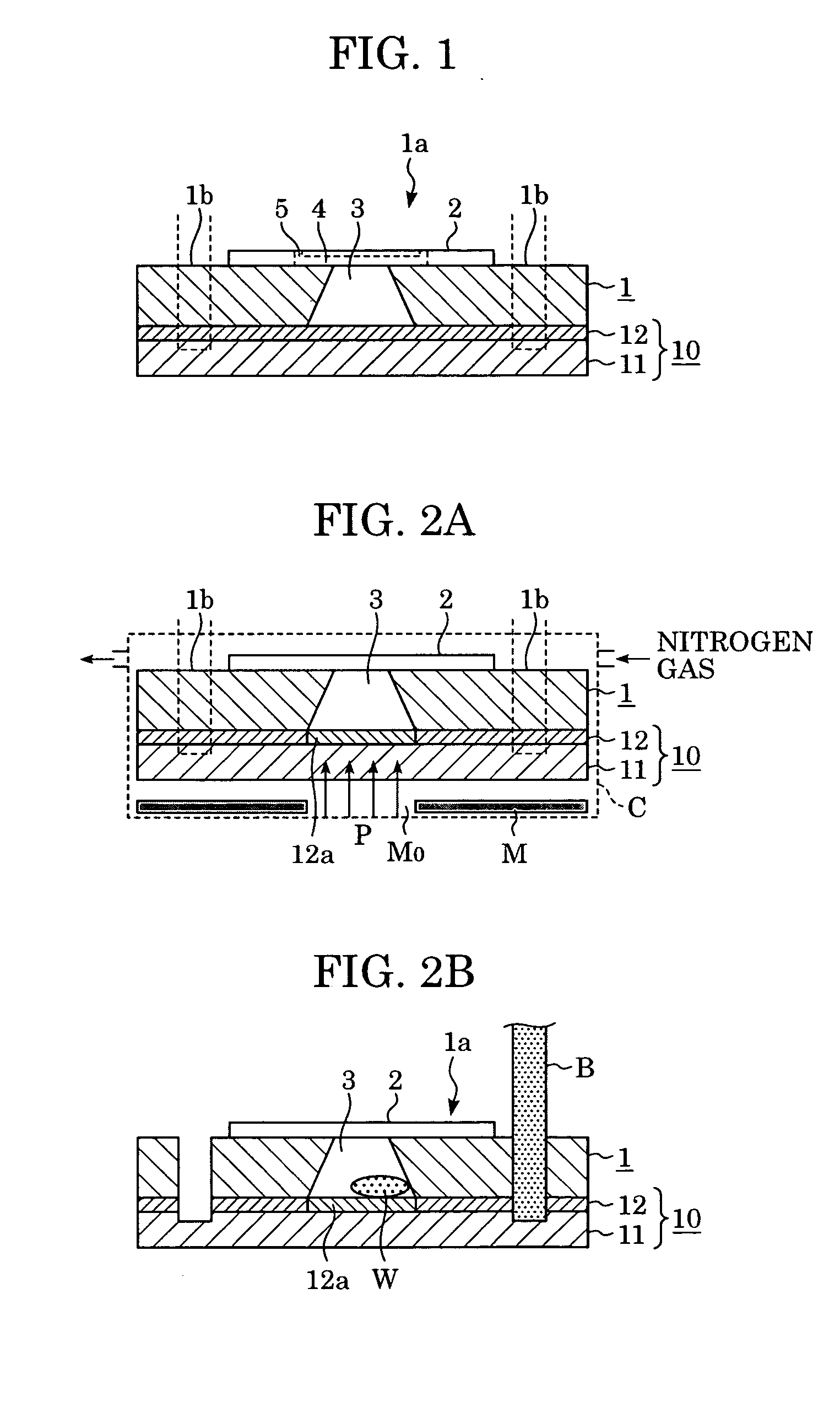
[0051] A first embodiment of the present invention provides a dicing method described below. With reference to FIG. 1, a wafer 1 to be diced has element sections 1a, which each include corresponding semiconductor circuit regions, nozzle layers 2 having orifices 5 and channels 4, and ink supply ports (liquid supply ports) 3. The semiconductor circuit regions and the nozzle layers 2 are arranged on the front face of the wafer 1 and form discharging devices. The liquid supply ports 3 extend from the rear face of the wafer 1 and communicate with the orifices 5 via the channels 4 placed therebetween. These components form element substrates for liquid-discharging heads. A dicing tape 10 including a bucking 11 and an adhesive 12 placed thereon is affixed to the rear face of the wafer 1. The element sections 1a are separated from each other by dicing the wafer 1 along dicing streets 1b extending along cutting lines. As shown in FIG. 2, before dicing is performed, ultraviolet light P is app...

second embodiment

[0072] A second embodiment of the present invention will now be described with reference to FIGS. 9 to 13.

[0073] In the first embodiment, the wafer 1 is loosely fixed during dicing after the adhesive 12 is partly cured prior to dicing. Therefore, minimum regions of the adhesive 12 are selectively cured. However, the width of the adhesive layers 12a that are formed by curing regions of the adhesive 12 as described above before dicing is performed increases with an increase in the dose (irradiation dose) of ultraviolet light; hence, the cured regions are apt to have a width greater than a required value. This phenomenon is referred to as an increase in pattern size and caused by the scattering of a portion of ultraviolet light incident on the backing 11. In general, in order to prevent an adhesive of a dicing tape from remaining on separated elements during the pick up of the elements, the adhesive has a thickness less than that of a backing. Therefore, ultraviolet light is mostly sc...

third embodiment

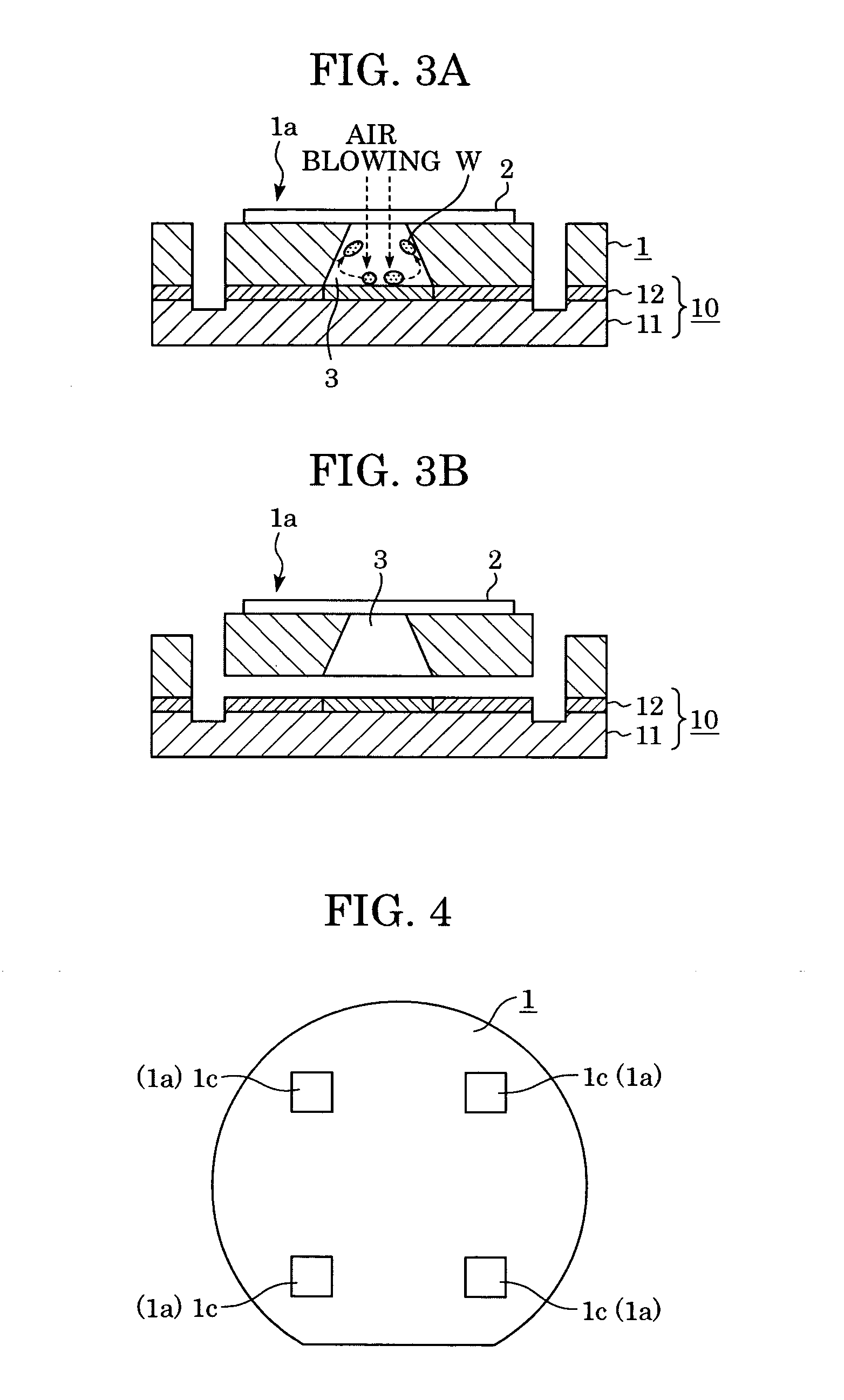
[0096] In the second embodiment, in order to prevent problems due to adhesive pieces derived from the dicing tape 10 from occurring, regions of the adhesive 12 that are exposed in the liquid supply ports 3 are cured and therefore reduced in adhesive strength before dicing is performed, whereby adhesive particles are created from the regions. Furthermore, it is necessary to prevent chippings from being created from portions of the adhesive 12 that correspond to the dicing streets 1b extending along cutting lines along which the wafer 1 is diced. In order to prevent such adhesive chippings from being created from the adhesive 12 subjected to dicing using a blade, the portions of the adhesive 12, which is included in the dicing tape 10, are cured before dicing is performed.

[0097] There are problems described below when the following regions and portions are simultaneously cured and therefore reduced in adhesive strength: the regions of the adhesive 12 that are exposed in the liquid su...


PUM

PropertyMeasurementUnit
Transmittivityaaaaaaaaaa

Abstract

A method for dicing a wafer having a first face in which opening are arranged along dicing streets. The method includes a step of affixing a dicing tape to the first face such that the dicing tape lies over the openings and adhesive regions of the dicing tape are exposed in the openings and a step of treating the dicing tape to reduce the adhesive strength of the adhesive regions.

Description

BACKGROUND OF THE INVENTION [0001] 1. Field of the Invention [0002] The present invention relates to methods for dicing wafers and particularly relates to methods for dicing wafers having semiconductor element sections arranged thereon to separate the semiconductor element sections. The present invention more particularly relates to a method for dicing a wafer having openings arranged in a face thereof and a dicing tape affixed to the wafer face to manufacture element substrates for liquid-discharging heads for discharging liquid from orifices arranged on the front faces of the substrates, the liquid being supplied from supply ports placed on the rear faces of the substrates. The present invention also relates to a method for manufacturing a liquid-discharging head using the dicing method. [0003] 2. Description of the Related Art [0004] In general, various semiconductor elements are manufactured by the following procedure: a plurality of semiconductor circuit sections are simultaneo...

Claims


Application Information

Patent Timeline
IPC IPC(8): B41J2/16H01L21/00
CPCB41J2/1603B41J2/1632H01L21/67092Y10S438/976Y10T156/1082Y10T156/1062Y10T156/1064Y10T156/1158
Inventor IRI, JUNICHIROKASHINO, TOSHIOINADA, GENJI
Owner CANON KK
Why Eureka
Try Eureka