
Semiconductor memory device with MOS transistors, each including a floating gate and a control gate, and a memory card including the same

a technology of mos transistor and memory card, which is applied in the direction of transistors, digital storage, instruments, etc., can solve the problems of difficult to reduce the size of the peripheral circuit around the memory cell array, particularly the size of the decoder circui

Inactive Publication Date: 2005-11-03
KK TOSHIBA
View PDF2 Cites 39 Cited by
  • Summary
  • Abstract
  • Description
  • Claims
  • Application Information

AI Technical Summary

Benefits of technology

[0010] According to an aspect of the present invention, there is provided a semiconductor memory device comprising: memory cells which include memory cell transistors, each of the transistors having a floating gate and a control gate; a memory cell array in which the memory cells are arranged in a matrix; bit lines each of which connects in common the drains of the memory cell transistors in a same column electrically; word lines each of which connects in common the control gates of the memory cell transistors in a same row; latch circuits which are provided for the bit lines in a one-to-one correspondence and which hold write data; a voltage generator which generates a negative voltage and a positive voltage; first row decoders which are pr...

Problems solved by technology

However, it has been difficult to reduce the size of the peripheral circuits around the memory cell array, particularly the size of the decoder circuits.

Method used


Image

  • Semiconductor memory device with MOS transistors, each including a floating gate and a control gate, and a memory card including the same
  • Semiconductor memory device with MOS transistors, each including a floating gate and a control gate, and a memory card including the same
  • Semiconductor memory device with MOS transistors, each including a floating gate and a control gate, and a memory card including the same

Examples


first embodiment

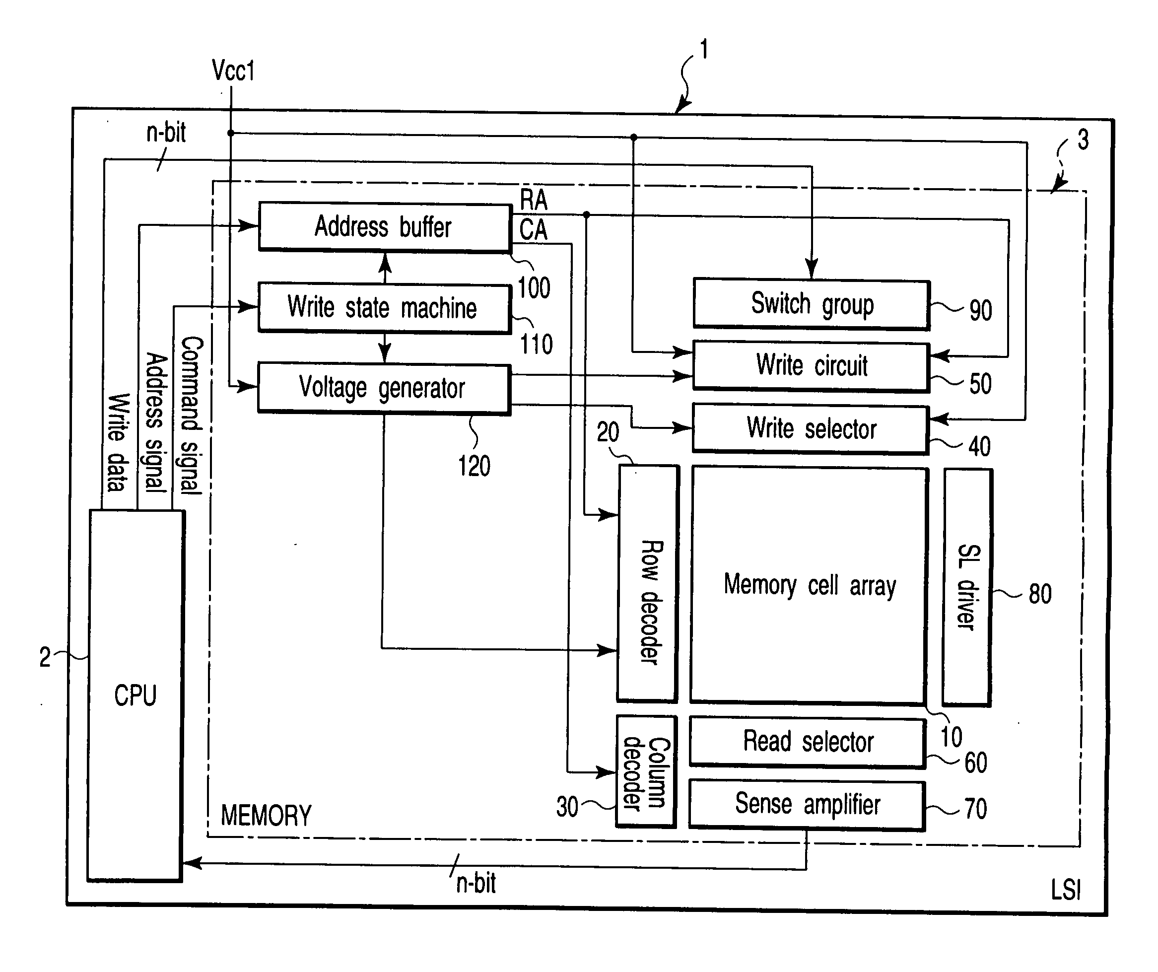
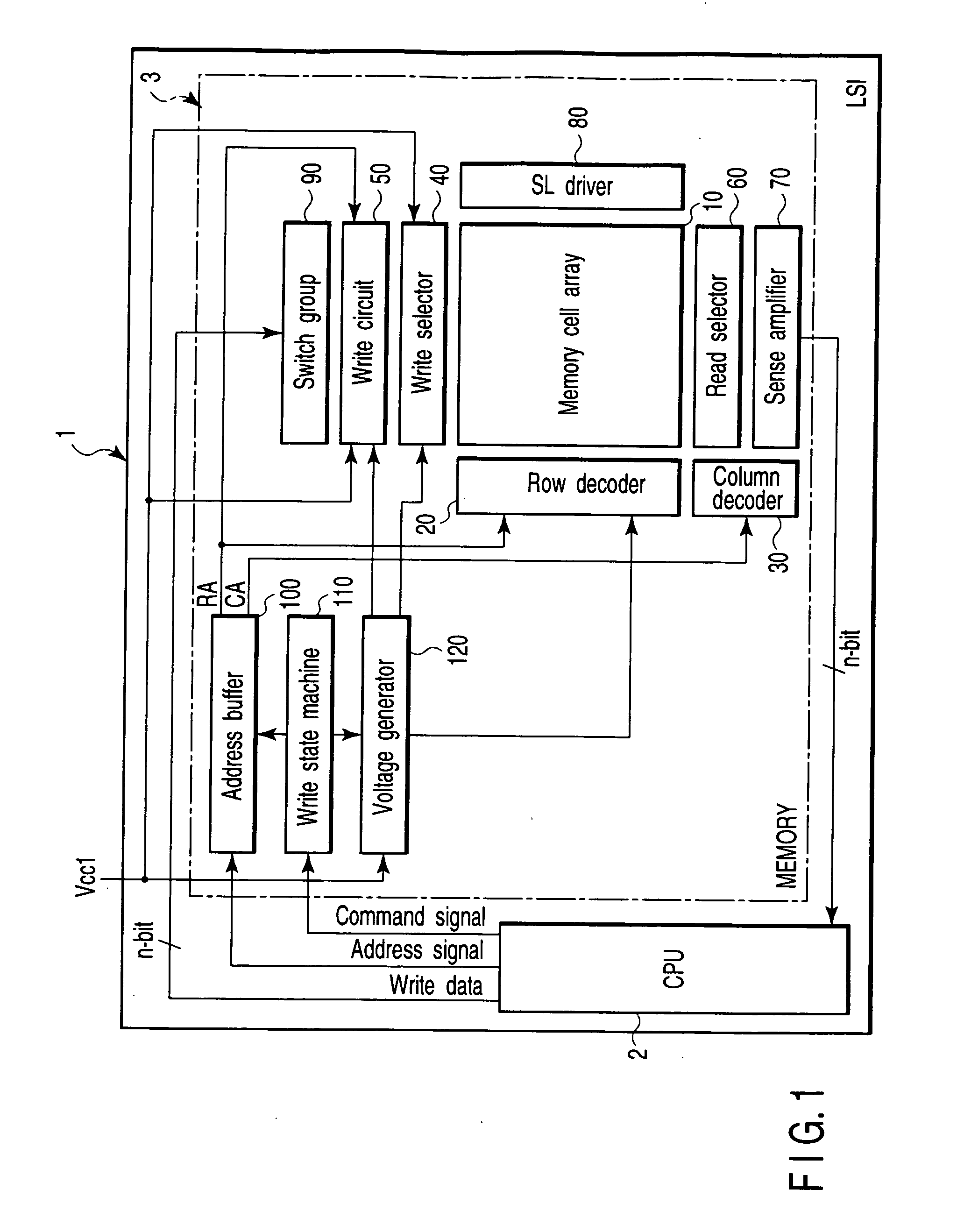
[0081] A semiconductor memory device according to the present invention will be explained by reference to FIG. 1.

[0082]FIG. 1 is a block diagram of a system LSI according to the first embodiment.

[0083] As shown in FIG. 1, the system LSI 1 comprises a CPU 2 and a 3Tr-NAND flash memory 3. The CPU 2 exchanges data with the flash memory 3. The flash memory 3 comprises a memory cell array 10, a row decoder 20, a column decoder 30, a write selector 40, a write circuit 50, a read selector 60, a sense amplifier 70, a source line driver 80, a switch group 90, an address buffer 100, a write state machine 110, and a voltage generator 120. A voltage of Vcc1 (about 3V) is externally applied to the LSI 1. The voltage Vcc is applied to the voltage generator 120, write circuit 50, and write selector 40.

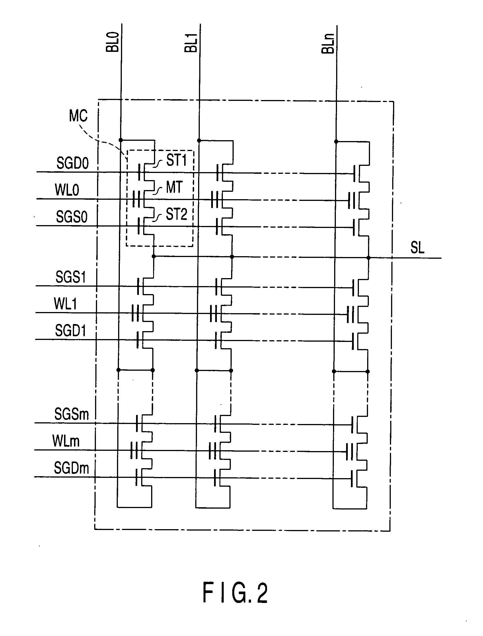
[0084] The memory cell array 10 has a plurality of memory cells arranged in a matrix. The configuration of the memory cell array 10 will be explained by reference to FIG. 2. FIG. 2 is a circuit dia...

second embodiment

[0232] The second embodiment further produces the following effects in item (7) and item (8). (7) The operation reliability of the flash memory can be improved.

[0233] With the second embodiment, the first row decoder 130 supplies the positive voltage and the second row decoder 140 supplies the negative voltage in an erase operation and a write operation. Therefore, in an erase operation, the same voltage as the potential VPW at the p-well region where the memory cells are formed can be applied to the unselected word lines. As a result, almost no voltage stress is applied to the gate insulating films of the memory cell transistors connected to the unselected word lines. Consequently, the deterioration of the gate insulating films of the memory cell transistors can be prevented.

[0234] Furthermore, in a write operation, the same voltage as the potential VPW can be applied to the unselected word lines. Applying the voltage directly to the unselected word lines without coupling suppress...

fourth embodiment

[0288] As shown in FIG. 48, a memory cell of the fourth embodiment has four values, “00,”“01,”“10,” and “11.” The threshold voltage of a memory cell with “11” data and that of a memory cell with “10” data are negative, whereas the threshold voltage of a memory cell with “01” data and that of a memory cell with “00” data are positive.

[0289] A method of setting a plurality of threshold voltages in memory cells may be as disclosed in, for example, Jpn. Pat. Appln. KOKAI Publication No. 2001-93288. In the publication, the threshold values of the memory cells are set by using only positive voltages. In the fourth embodiment, however, the negative voltages supplied from the first and row decoders 130, 140 are used in a write and a verify operation as shown in FIG. 49. This makes it possible to set negative threshold voltages.

[0290] As described above, the NAND flash memory of the fourth embodiment produces not only the effects explained in the third embodiment but also the effect in the ...


PUM

PropertyMeasurementUnit
Electric potential / voltageaaaaaaaaaa
Lengthaaaaaaaaaa
Electrical conductivityaaaaaaaaaa

Abstract

A semiconductor memory device includes memory cells, a memory cell array, word lines, latch circuits, first row decoders, second row decoders, first isolating transistors, and second isolating transistors. The memory cell includes a memory cell transistor having a floating gate and a control gate. The memory cell array includes the memory cells arranged in a matrix. The word line connects in common the control gates of the memory cell transistors in a same row. The first row decoder applies a positive voltage to the word lines in a write operation and in an erase operation. The second row decoder applies a negative voltage to the word lines in a write operation and in an erase operation. The first isolating transistor switches between the first row decoder and the word line. The second isolating transistor switches between the second row decoder and the word line.

Description

CROSS-REFERENCE TO RELATED APPLICATIONS [0001] This application is based upon and claims the benefit of priority from prior Japanese Patent Application No. 2004-134672, filed Apr. 28, 2004, the entire contents of which are incorporated herein by reference. BACKGROUND OF THE INVENTION [0002] 1. Field of the Invention [0003] This invention relates to a semiconductor memory device with MOS transistors, each including a floating gate and a control gate, and to a memory card including the semiconductor memory device. More particularly, this invention relates to a nonvolatile semiconductor memory device, such as a flash memory. [0004] 2. Description of the Related Art [0005] Various types of flash memories have been proposed for a variety of uses. [0006] For instance, a NAND flash memory has been known as a data storage memory for use in a digital camera or the like. A NAND flash memory has been described in, for example, Imamiya K., et al., “A 125-mm / sup 2 / 1-Gb NAND Flash Memory With 10-...

Claims


Application Information

Patent Timeline
IPC IPC(8): G11C16/06G11C11/34G11C16/02G11C16/04G11C16/08G11C16/12G11C16/26H01L21/8247H01L27/10H01L27/115H01L29/788H01L29/792
CPCG11C11/5628G11C11/5642G11C16/26G11C16/08G11C16/12G11C16/0483
Inventor UMEZAWA, AKIRA
Owner KK TOSHIBA
Learn More