Overlay box structure for measuring process induced line shortening effect

a lithographic structure and overlay box technology, applied in the field of semiconductor processing, can solve the problems removing wafers may not be suitable for production materials, etc., and achieve the effect of reducing the throughput time in the fabrication of wafers and increasing the cos

Inactive Publication Date: 2005-11-10
NXP BV
View PDF6 Cites 5 Cited by
  • Summary
  • Abstract
  • Description
  • Claims
  • Application Information

AI Technical Summary

Benefits of technology

[0015] In an example semiconductor process, in gauging the quality of the printing of the CDs in a wafer process, a Scanning Electron Microscope (SEM) is used to measure the lines and space that define CDs. However, the use of a SEM reduces the throughput time in the wafer fabrication, in that the wafer substrate is removed from the production flow. Furthermore, the removed wafer may be unsuitable for production material after SEM analysis. There exists a need for a way to obtain the CD information that does not adversely affect throughput time resulting in additional cost.

Problems solved by technology

However, the use of a SEM reduces the throughput time in the wafer fabrication, in that the wafer substrate is removed from the production flow.
Furthermore, the removed wafer may be unsuitable for production material after SEM analysis.

Method used


Image

  • Overlay box structure for measuring process induced line shortening effect
  • Overlay box structure for measuring process induced line shortening effect
  • Overlay box structure for measuring process induced line shortening effect

Examples


Embodiment Construction

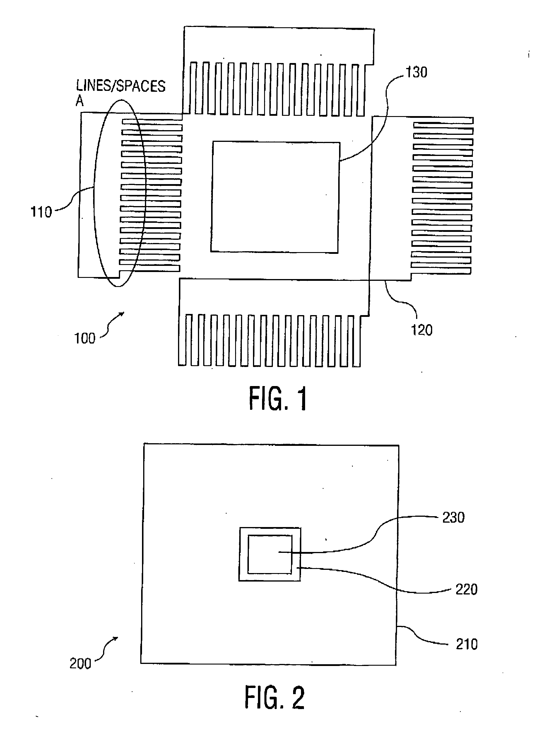
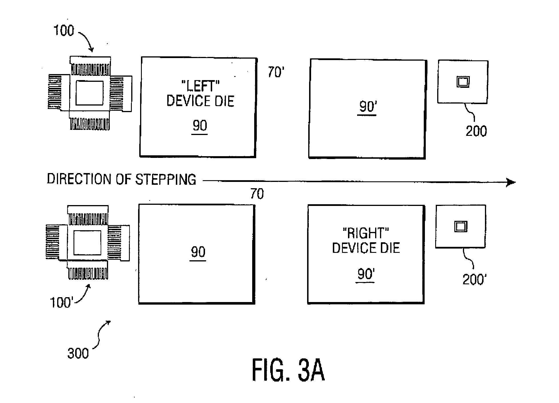
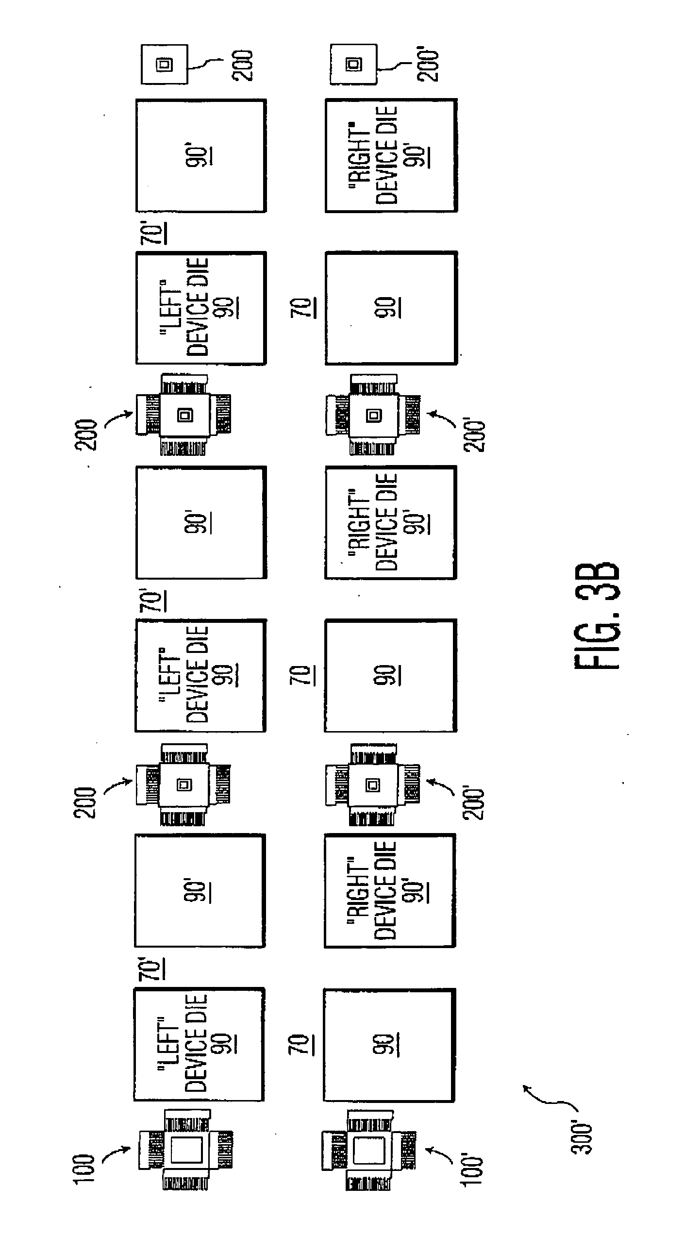
[0037] The present invention has been found to be useful in the measuring of actual line shortening width using an overlay measurement tool. End of line shortening as observed in a lithographic process is well known. The effect is due to the diffraction of light passing through the corners of open spaces in the reticle. Because of diffraction, the aerial image at the mask edge is steeper and more faithful along the line compared to that on the end of the line. At best focus in the process, there is still some line shortening, though minimized. As focus goes outward from the best focus in either a positive or negative direction, the amount of line shortening increases. Further discussion of line shortening may be found in the paper titled, “Understanding Optical End of Line Metrology” (Optical Engineering, Vol. 39. No. 7, July 2000, Pages 1951-1957)” by David Ziger and Pierre Leroux, which is herein incorporated by reference in its entirety.

[0038] In wafer fabrication, the user may ...


PUM

PropertyMeasurementUnit
wavelengthaaaaaaaaaa

Abstract

The present invention enables the user to measure process line shortening (PLS) on an overlay tool. In an example embodiment (900), to obtain the PLS, the user applies a method to determine the misalignment (MA) of a composite image on a substrate (940a), from the composite image the user may determine the total line (940b) shortening (TLS) and the equipment line (940c) shortening (ELS). The process line shortening (PLS) is determined (940d) as a function of TLS and ELS.

Description

RELATED APPLICATION [0001] This application is being filed concurrently with an application (Attorney Docket No. US 030109) titled, “A Method and Lithographic Structure for Measuring Lengths of Lines and Spaces,” of Yuji Yamaguchi, the application assigned to Koninklijke Philips Electronics N.V. of The Netherlands, the application is incorporated by reference in its entirety. FIELD OF THE INVENTION [0002] The invention relates to semiconductor processing. More particularly the invention relates to the measuring of lengths of lines and spaces with lithographic structures. BACKGROUND [0003] The electronics industry continues to rely upon advances in semiconductor technology to realized higher-function devices in more compact areas. For many applications, realizing higher-functioning devices requires integrating a large number of electronic devices into a single silicon wafer. As the number of electronic devices per given area of the silicon wafer increases, the manufacturing process b...

Claims


Application Information

Patent Timeline
Patent Type & Authority Applications(United States)
IPC IPC(8): G03C5/00G03F7/20G03F9/00G06K9/00
CPCG03F7/70441G03F7/70683G03F7/70633
Inventor YAMAGUCHI, YUJILEROUX, PIERRE
Owner NXP BV
Why Eureka
Try Eureka