Method for fabricating semiconductor device with recessed channel region

Inactive Publication Date: 2005-11-10
SK HYNIX INC
View PDF3 Cites 9 Cited by
  • Summary
  • Abstract
  • Description
  • Claims
  • Application Information

AI Technical Summary

Benefits of technology

[0018] It is, therefore, an object of the present invention to provide a method for fabricating a semiconductor device with a plurality of recessed channel

Problems solved by technology

Also, there is a problem of making a depth of the plurality of moats M deeper by being additionally wet

Method used


Image

  • Method for fabricating semiconductor device with recessed channel region
  • Method for fabricating semiconductor device with recessed channel region
  • Method for fabricating semiconductor device with recessed channel region

Examples


Example

[0025] A method for fabricating a semiconductor device with a plurality of recessed channel regions in accordance with a preferred embodiment of the present invention will be described in detail with reference to the accompanying drawings.

[0026]FIGS. 3A to 3E are cross-sectional views illustrating a method for forming a semiconductor device by using a recessed channel array transistor (RCAT) technology in accordance with the present invention.

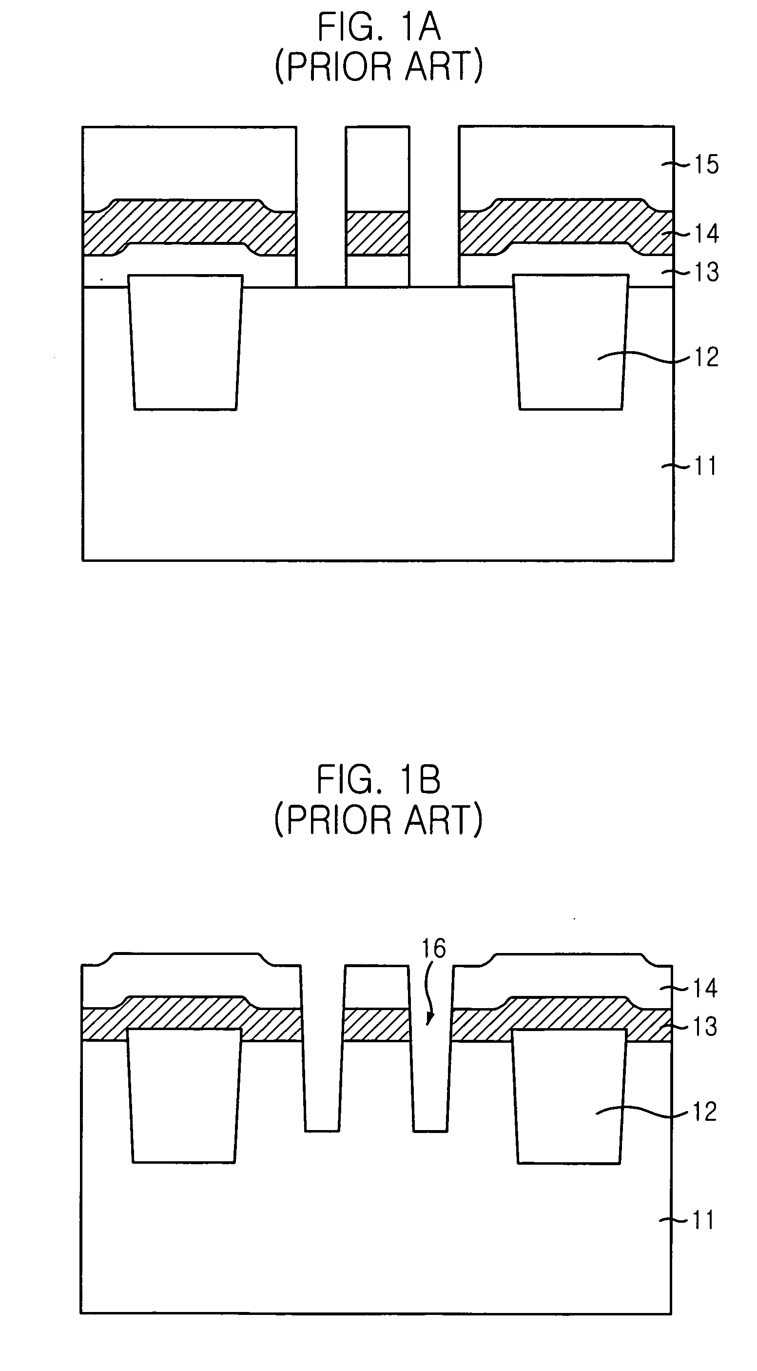
[0027] Referring to FIG. 3A, a plurality of device isolation layers for a plurality of trenches 22 are formed on a substrate 21 and then, a hard mask nitride layer 23 is formed on the substrate 21.

[0028] At this time, the hard mask nitride layer 23 is formed with silicon nitride (Si3N4) in a thickness ranging from approximately 50 Å to approximately 200 Å.

[0029] Next, a hard mask oxide layer 24 and a hard mask polysilicon layer 25 are sequentially deposited on the hard mask nitride layer 23. Herein, the hard mask oxide layer 24 is made of s...


PUM


Abstract

Disclosed is a method for fabricating a semiconductor device with a plurality of recessed channel regions. This method includes the steps of: forming a plurality of device isolation layers in a substrate; forming a hard mask nitride layer, a hard mask oxide layer and a hard mask polysilicon layer on the device isolation and the substrate, thereby obtaining a hard mask pattern; forming a plurality of trenches in the predetermined regions of the substrate with use of the hard mask pattern to expose a plurality of recessed channel regions; selectively removing the hard mask pattern; and forming a plurality of gate structures in the plurality of trenches.

Description

FIELD OF THE INVENTION [0001] The present invention relates to a method for fabricating a semiconductor device; and more particularly, to a method for fabricating a semiconductor using a recessed channel array transistor (RCAT) technology. DESCRIPTION OF RELATED ARTS [0002] As a scale of integration and fineness of a semiconductor device has increased, required process capability and reliability have been increased as well. Especially, in case of a dynamic random access memory (DRAM), a property of a transistor is determined by a shallow trench isolation (STI) process and a process for forming a gate structure. This property of the transistor is the most important factor to determine overall stability of the DRAM. Accordingly, it should be secured to improve stability of the STI process and the process for forming the gate structure to increase the overall reliability of the DRAM. [0003] The STI process is one of the device isolation methods of a semiconductor device. That is, a tre...

Claims


Application Information

Patent Timeline
IPC IPC(8): H01L21/00H01L29/78H01L21/335H01L21/336H01L21/76H01L21/8234H01L21/8242
CPCH01L21/823425H01L21/823437H01L29/7834H01L29/66621H01L27/10873H10B12/05E03C1/2302
Inventor PARK, SOO-YOUNG
Owner SK HYNIX INC
Why Eureka
Try Eureka