

Flip chip package and process of forming the same
a chip and chip technology, applied in the field of flip chip packages, can solve the problems of failure of the circuit substrate, damage to the aesthetic appearance of the package, etc., and achieve the effect of maintaining the aesthetic appearance of the circuit substrate and reducing the possibility of fiducial marks
- Summary
- Abstract
- Description
- Claims
- Application Information
AI Technical Summary
Benefits of technology
Problems solved by technology
Method used
Image

Examples
Embodiment Construction
[0024] Reference will now be made in detail of the present preferred embodiments of the invention, examples of which are illustrated in the accompanying drawings. Wherever possible, the same reference numbers are used in the drawings and the description to refer to the same or like parts.
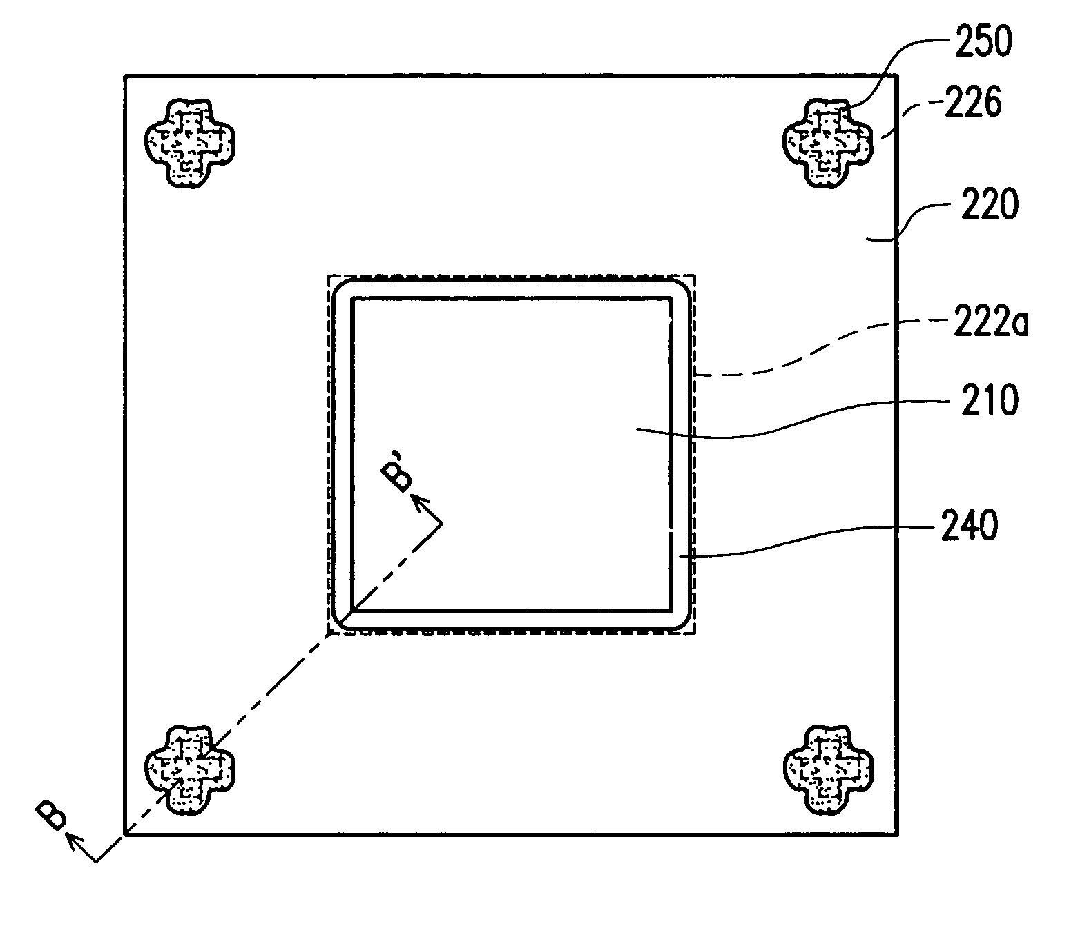
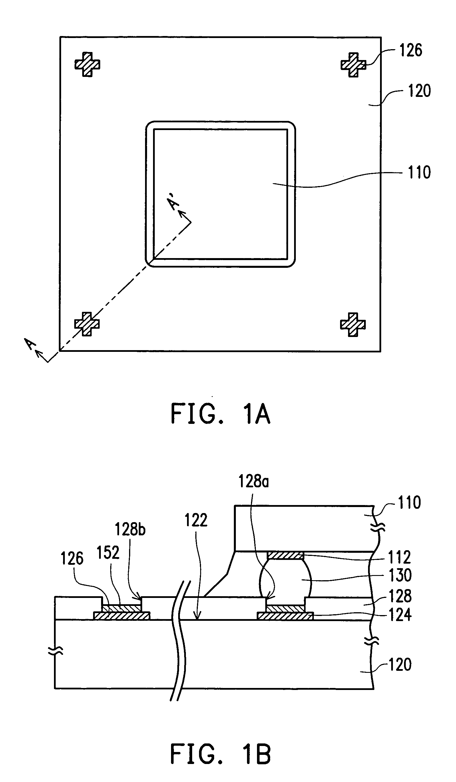
[0025] Referring to FIGS. 4A, 4B and 5, wherein FIG. 4A is the bottom view of a flip chip package in accordance with an embodiment of the present invention, FIG. 4B is a sectional view along B-B′ of FIG. 4A, and FIG. 5 is a flowchart of a first flip chip package process in accordance with an embodiment of the present invention.
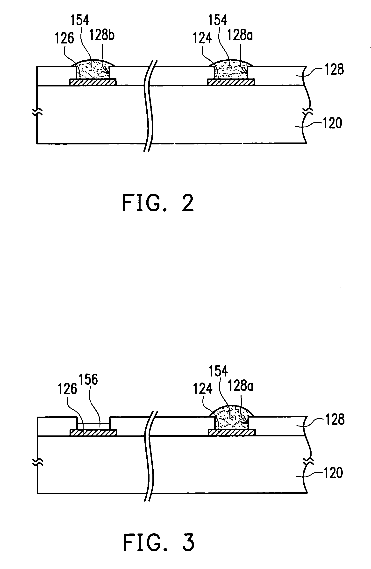
[0026] As shown at step 510, a chip 210 is connected to a circuit substrate 220 by a flip chip interconnect method. The circuit substrate 220 has a carrier surface 222, a plurality of bump pads 224 (only one being shown), and a plurality of fiducial marks 226. The carrier surface 222 has a chip connection region 222a, wherein the bump pads 224 are disposed on the chip connec...
PUM
 Abstract
Description
Claims
Application Information