
Lithographic apparatus and device manufacturing method

a technology of lithographic apparatus and manufacturing method, which is applied in the direction of electrical apparatus, printers, instruments, etc., can solve the problems of poor image quality, affecting imaging performance, and current models only being approximate and coars

Inactive Publication Date: 2005-11-17
ASML NETHERLANDS BV
View PDF7 Cites 39 Cited by
  • Summary
  • Abstract
  • Description
  • Claims
  • Application Information

AI Technical Summary

Benefits of technology

[0011] This apparatus and method of the invention are advantageous because they use actual measurements of the intensity distribution (also referred to as pupil filling) with the patterning device in situ, to provide improved prediction of the lens heating aberration effects. This improves the feed-forward correction and reduces the number of feed-back measurements which are required, thereby improving throughput.
[0014] In certain embodiments, information on the radiation intensity distribution can be obtained without inserting any additional tools or components into the apparatus. This means that the measurement can be rapid.
[0016] In certain embodiments, the method further includes determining the derivative of the irradiance measurements as a function of the numerical aperture to obtain information on the intensity distribution at a pupil plane of the projection system (i.e., pupil filling). This enables the pupil filling, azimuthally averaged, to be readily obtained.

Problems solved by technology
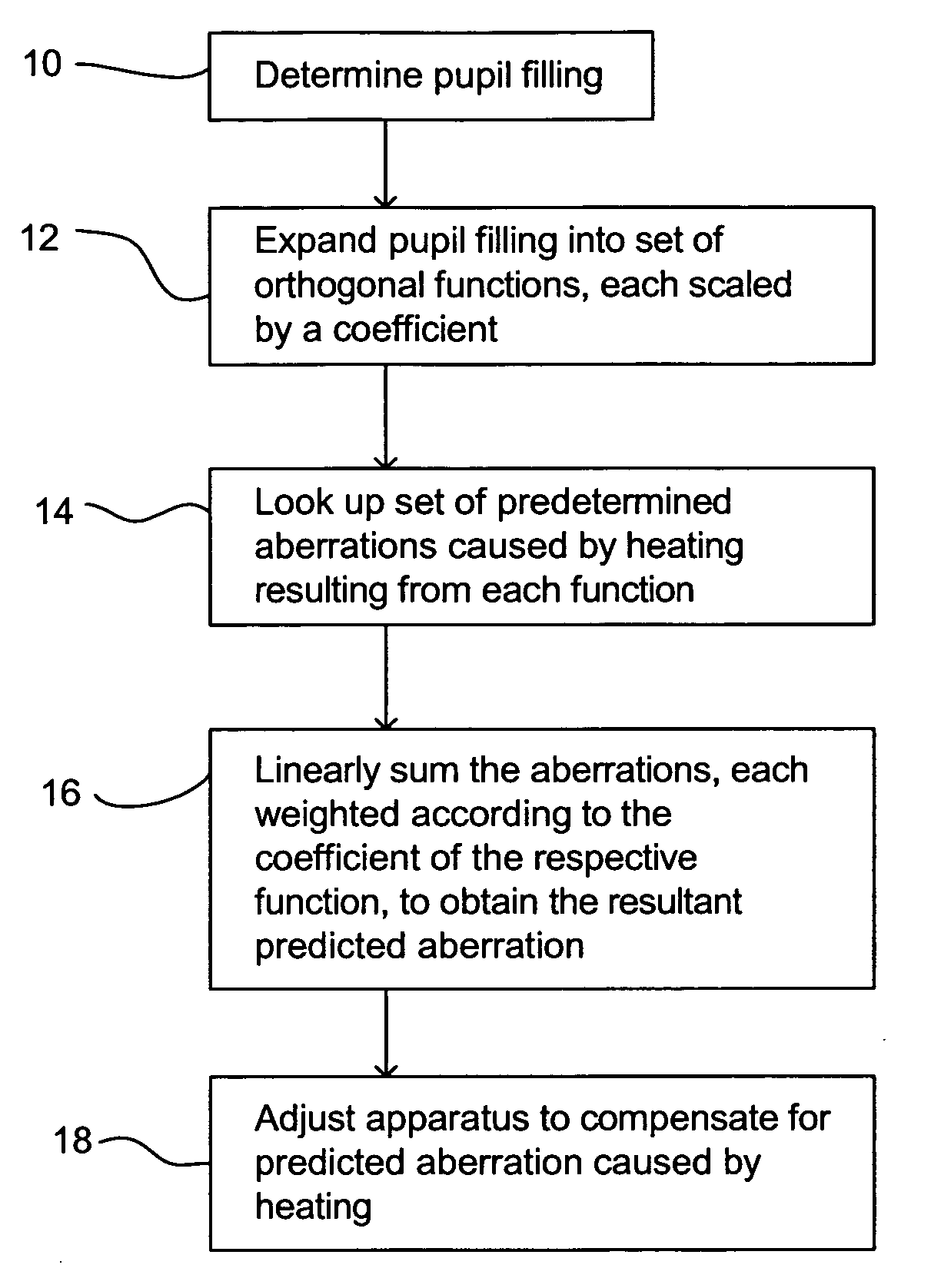
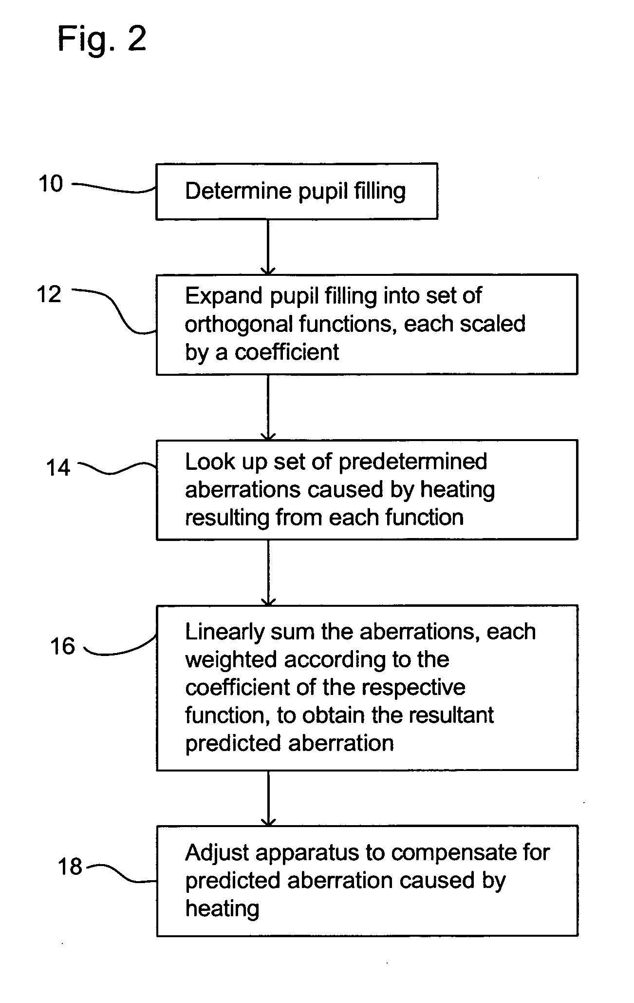
This causes heating of the projection lens which results in lens aberration and so is detrimental to the imaging performance.
However, current models are only approximate and coarse, for example only using the average reticle transmission, illumination mode and numerical aperture as parameters.
This excludes diffraction effects of the reticle and may also not be a valid model for more sophisticated reticles such as ones with differential attenuation and phase-shift masks.
This leads to large residual errors after the feed-forward model is applied.
However, these feed-back measurements result in a significant throughput penalty.
Another problem is that some chips can be very complex, for example with a DRAM part and a logic part.
There is a problem regarding how to include these effects in the feed-forward model; if they are not included, this can cause errors in the calculated aberration.
This can mean that the measurement is slow or indirect.
Measurement of the scanning pupil in a scanner has also been difficult.

Method used


Image

  • Lithographic apparatus and device manufacturing method
  • Lithographic apparatus and device manufacturing method
  • Lithographic apparatus and device manufacturing method

Examples


embodiment 1

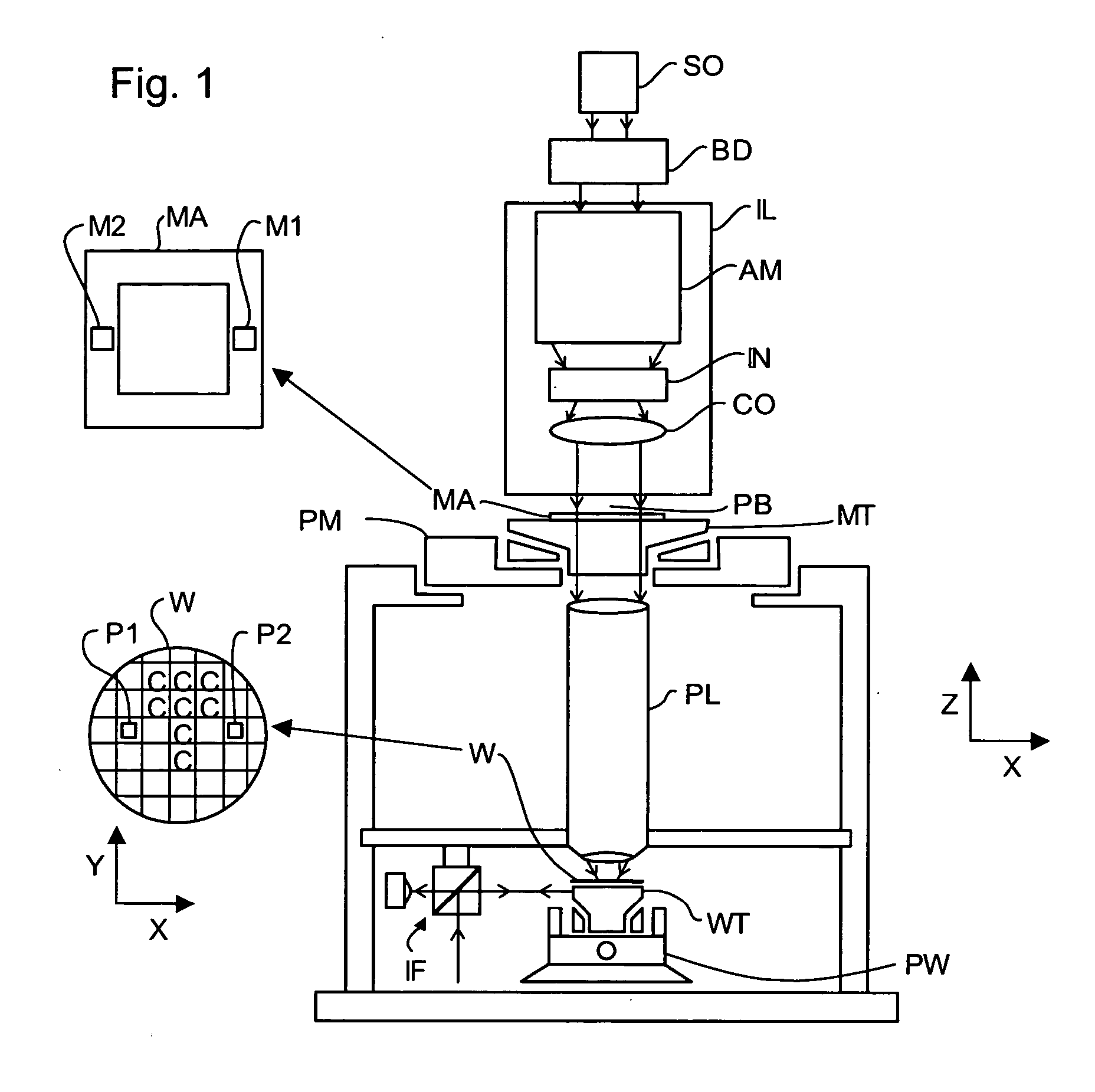
[0031]FIG. 1 schematically depicts a lithographic apparatus according to a particular embodiment of the invention. The apparatus includes: [0032] an illumination system (illuminator) IL for providing a projection beam PB of radiation (e.g., UV radiation or EUV radiation). [0033] a first support structure (e.g., a mask table) MT for supporting a patterning device (e.g., a mask) MA and connected to a first positioner PM for accurately positioning the patterning device with respect to item PL; [0034] a substrate table (e.g., a wafer table) WT for holding a substrate (e.g., a resist-coated wafer) W and connected to a second positioner PW for accurately positioning the substrate with respect to item PL; and [0035] a projection system (e.g., a refractive projection lens) PL for imaging a pattern imparted to the projection beam PB by the patterning device MA onto a target portion C (e.g., comprising one or more dies) of the substrate W.

[0036] As here depicted, the apparatus is of a transm...

embodiment 2

[0067] This embodiment of the invention concerns a method for determining information on the pupil of the projection lens. It may be used in some circumstances in conjunction with the preceding embodiment, or may be used independently.

[0068] This embodiment is for use with a lithographic apparatus in which the projection lens has an adjustable numerical aperture. FIG. 3 illustrates schematically the projection system comprising a projection lens PL, a cone of radiation 30 from the illuminator, a means for adjustably defining the numerical aperture such as an adjustable diaphragm 32, a cone of radiation 34 exiting the projection lens, and a sensor 36. FIG. 3 shows four different settings of the numerical aperture. The angular aperture is defined as the angle between the most divergent rays that can pass through the lens system to form the image and the numerical aperture (NA) is the sine of half the angular aperture.

[0069] The sensor 36 is, for example, a dose sensor already provid...


PUM

PropertyMeasurementUnit
wavelengthaaaaaaaaaa

Abstract

A lithographic apparatus includes an instrument for determining the radiation intensity distribution at a pupil plane of the projection system while a patterning device is imparting the projection beam with a pattern, a calculation apparatus for calculating the effect on the imaging by the projection system of heating resulting from the projection beam in the projection system having the determined intensity distribution and a controller for adjusting the lithographic apparatus to compensate for the calculated effect of heating.

Description

BACKGROUND OF THE INVENTION [0001] 1. Field of the Invention [0002] The present invention relates to a lithographic apparatus and a device manufacturing method. [0003] 2. Discussion of Related Art [0004] A lithographic apparatus is a machine that applies a desired pattern onto a target portion of a substrate. Lithographic apparatus can be used, for example, in the manufacture of integrated circuits (ICs). In that circumstance, a patterning device, such as a mask, may be used to generate a circuit pattern corresponding to an individual layer of the IC, and this pattern can be imaged onto a target portion (e.g., comprising part of, one or several dies) on a substrate (e.g., a silicon wafer) that has a layer of radiation-sensitive material (resist). In general, a single substrate will contain a network of adjacent target portions that are successively exposed. Known lithographic apparatus include so-called steppers, in which each target portion is irradiated by exposing an entire patte...

Claims


Application Information

Patent Timeline
Patent Type & Authority Applications(United States)
IPC IPC(8): G03B27/52H01L21/027G03F7/20
CPCG03F7/70891G03F7/70133
Inventor MARIE VAN GREEVENBROEK, HENDRIKUS ROBERTUSLUDOVICUS VAN DIJCK, HENDRIKUS ALPHONSUSWAGNER, CHRISTIANJORRITSMA, LAURENTIUS CATRINUS
Owner ASML NETHERLANDS BV
Learn More