Flash memory device and method for driving the same

a flash memory and memory device technology, applied in lighting applications, lighting and heating apparatus, instruments, etc., can solve the problems of increasing heterogeneity of program threshold voltage, low program speed, and disadvantages of program speed, so as to reduce program or erase time

Active Publication Date: 2005-11-17
STMICROELECTRONICS SRL +1
View PDF5 Cites 17 Cited by
  • Summary
  • Abstract
  • Description
  • Claims
  • Application Information

AI Technical Summary

Benefits of technology

[0010] The present invention is directed to a flash memory device which can reduce a program or erase time by varying an initial pulse width or an initial bias level in a program or erase operation using an ISPP scheme, and a method for driving the same.

Problems solved by technology

The NOR type nonvolatile memory device programs data of eight memory cells at a time in byte units, namely, in parallel due to current restrictions, and thus is disadvantageous in program speed.
Therefore, in a repetitive application method of simple program pulses having the same pulse voltage value and the same pulse time width, the program and verify operations must be performed about 100 times. In this case, a time taken to convert a voltage of the program and verify operations is much longer than a time taken to apply a program voltage, which results in a low program speed.
However, the memory cell having the highest program speed is over-programmed, thereby increasing heterogeneity of a program threshold voltage.

Method used


Image

  • Flash memory device and method for driving the same
  • Flash memory device and method for driving the same
  • Flash memory device and method for driving the same

Examples


Embodiment Construction

[0021] A flash memory device and a method for driving the same in accordance with a preferred embodiment of the present invention will now be described in detail with reference to the accompanying drawings.

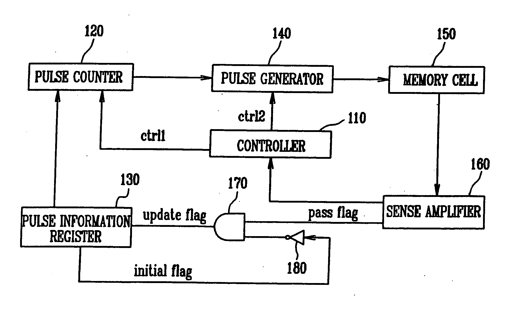
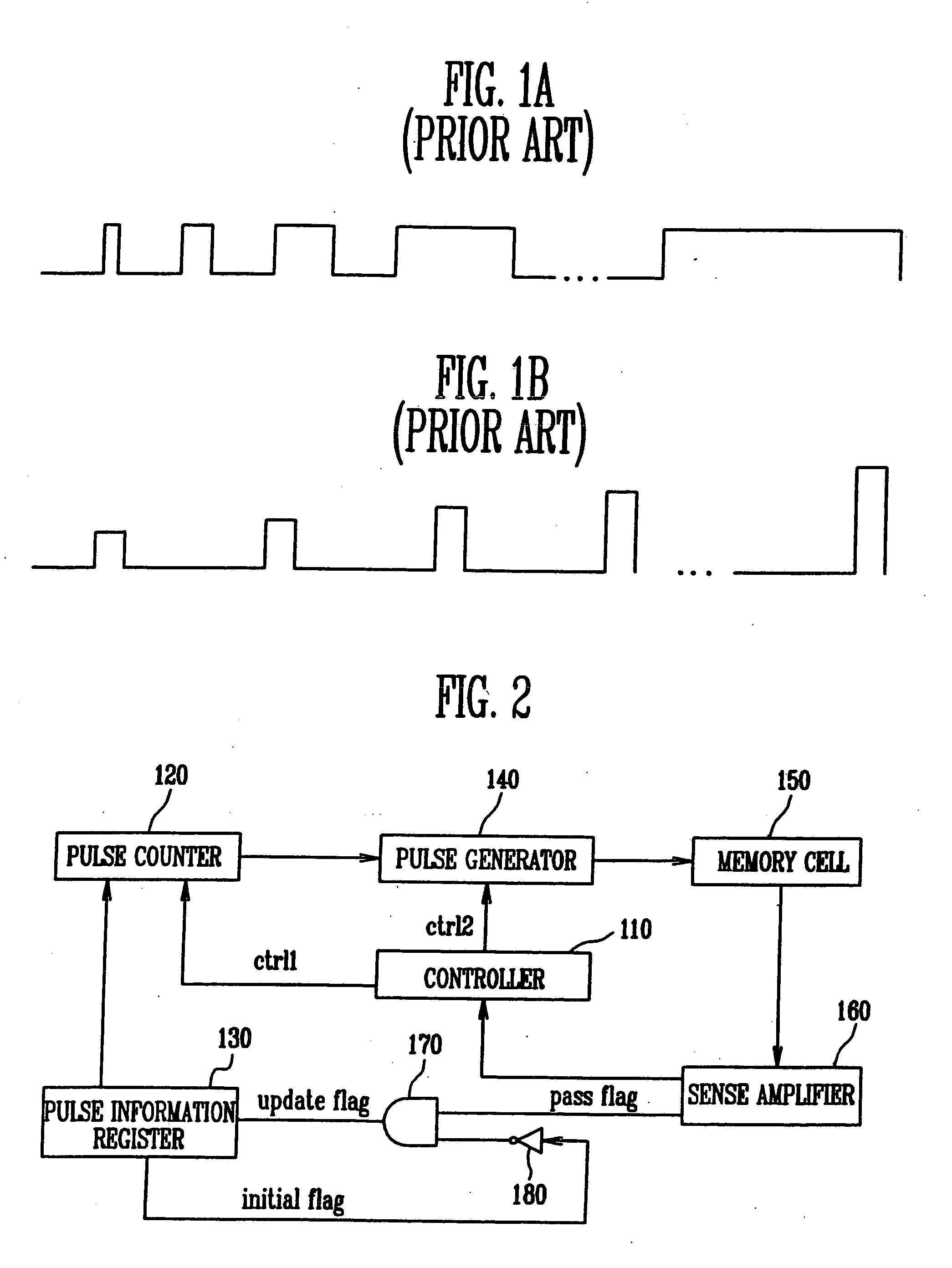
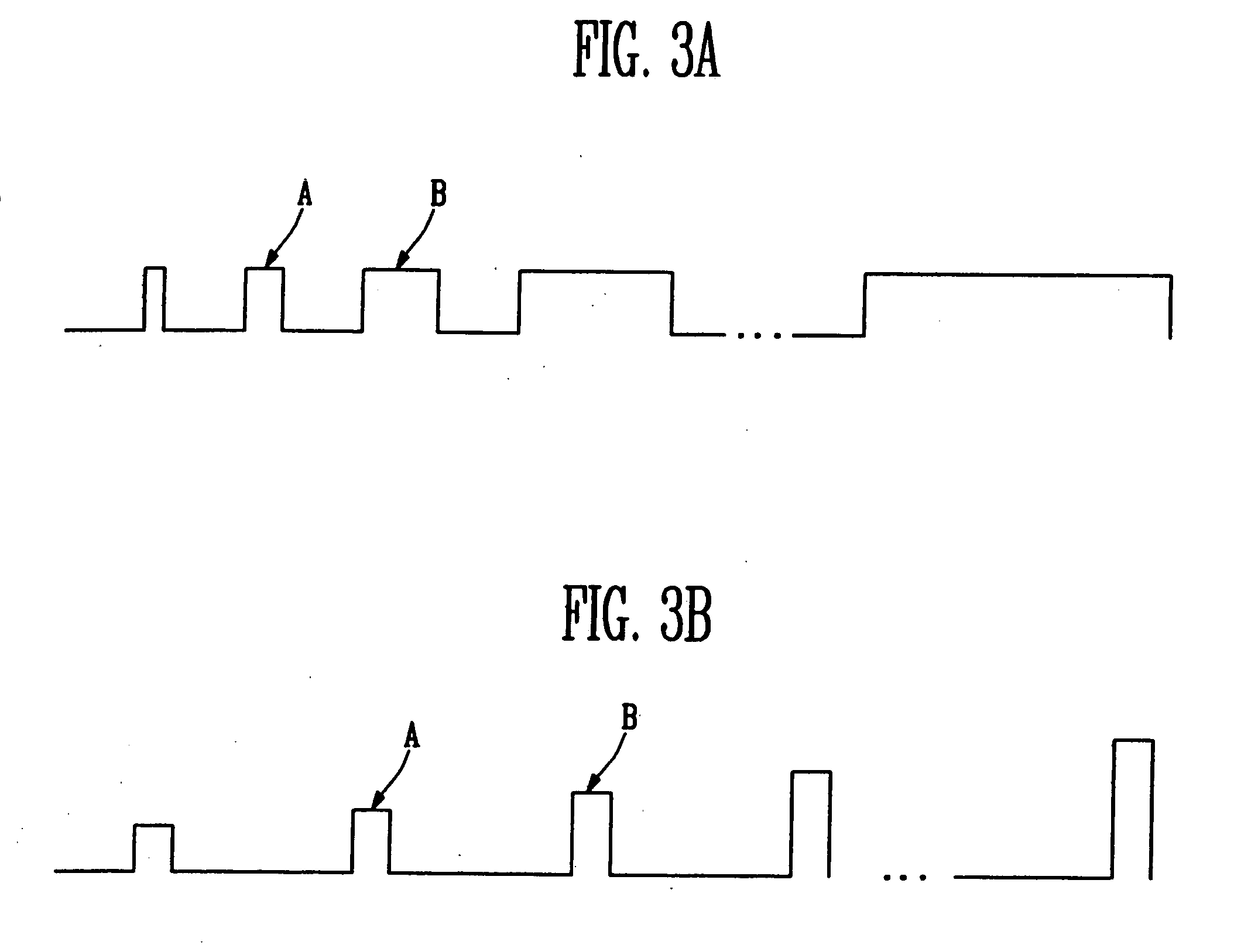
[0022]FIG. 2 is a block diagram illustrating the structure of the flash memory device in accordance with the present invention. The flash memory device can reduce the whole program or erase time, by storing a pulse width or a bias level for passing at least one bit of cells of one page in a program or erase operation using an ISPP scheme, and using the stored pulse width or bias level as an initial pulse width or an initial bias level in a succeeding program or erase operation.

[0023] A pulse information register 130 stores initial pulse width or initial bias level information. A controller 110 generates a first control signal ctrl1 according to a program or erase command, so that a pulse counter 120 can receive the initial pulse width or initial bias level information from the p...


PUM


Abstract

A flash memory device which can reduce the whole program or erase time and improve reliability by cycling, by storing a pulse width or a bias level for passing at least one bit of cells of a first page in a program or erase operation using an ISPP scheme, and using the stored pulse width or bias level as an initial pulse width or an initial bias level in a succeeding program operation or erase operation, and a method for driving the same.

Description

BACKGROUND [0001] 1. Field of the Invention [0002] The present invention relates to a flash memory device and a method for driving the same, and more particularly to, a flash memory device which can reduce a program or erase time by varying an initial pulse width or an initial bias level in a program or erase operation using an Incremental Step Pulse Programming (ISPP) scheme, and a method for driving the same. [0003] 2. Discussion of Related Art [0004] Among nonvolatile memory devices such as an Electrically Erasable and Programmable Read Only Memory (EEPROM) and a flash memory, a NOR type nonvolatile memory device which performs a data program operation by injecting electrons into a floating gate by channel hot electron injection has been widely used. The NOR type nonvolatile memory device programs data of eight memory cells at a time in byte units, namely, in parallel due to current restrictions, and thus is disadvantageous in program speed. [0005] Recently, a NAND type flash mem...

Claims


Application Information

Patent Timeline
Patent Type & Authority Applications(United States)
IPC IPC(8): G11C16/04G11C16/02G11C16/10G11C16/32G11C16/34G11C29/00
CPCG11C16/10G11C16/3436G11C16/32F21L14/02F21V15/01F21V17/104F21W2131/402
Inventor WANG, JONG HYUN
Owner STMICROELECTRONICS SRL
Why Eureka
Try Eureka