

Apparatus and method for detecting defect and apparatus and method for extracting wire area
a technology of defect detection and apparatus, applied in image data processing, instruments, image enhancement, etc., to achieve the effect of removing the noise caused by the inspection binary imag
- Summary
- Abstract
- Description
- Claims
- Application Information
AI Technical Summary
Benefits of technology
Problems solved by technology
Method used
Image

Examples
Embodiment Construction
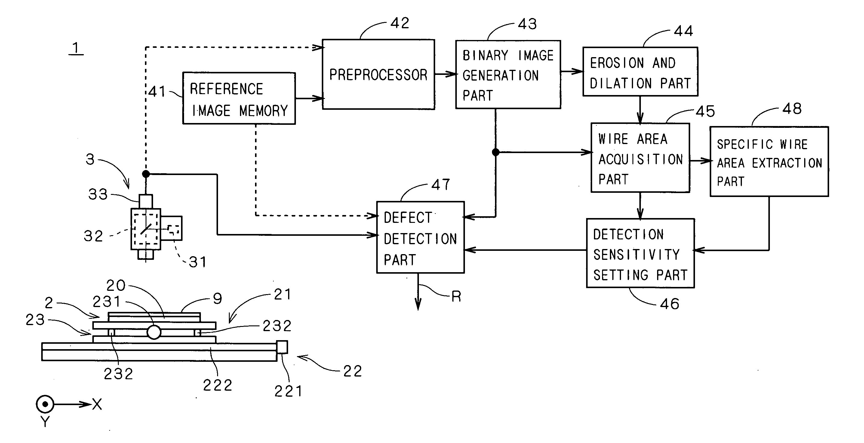
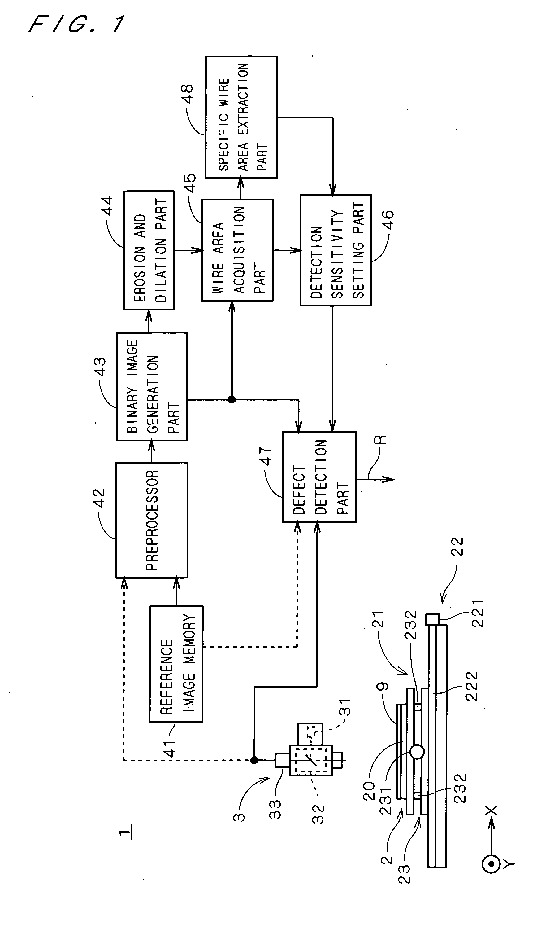
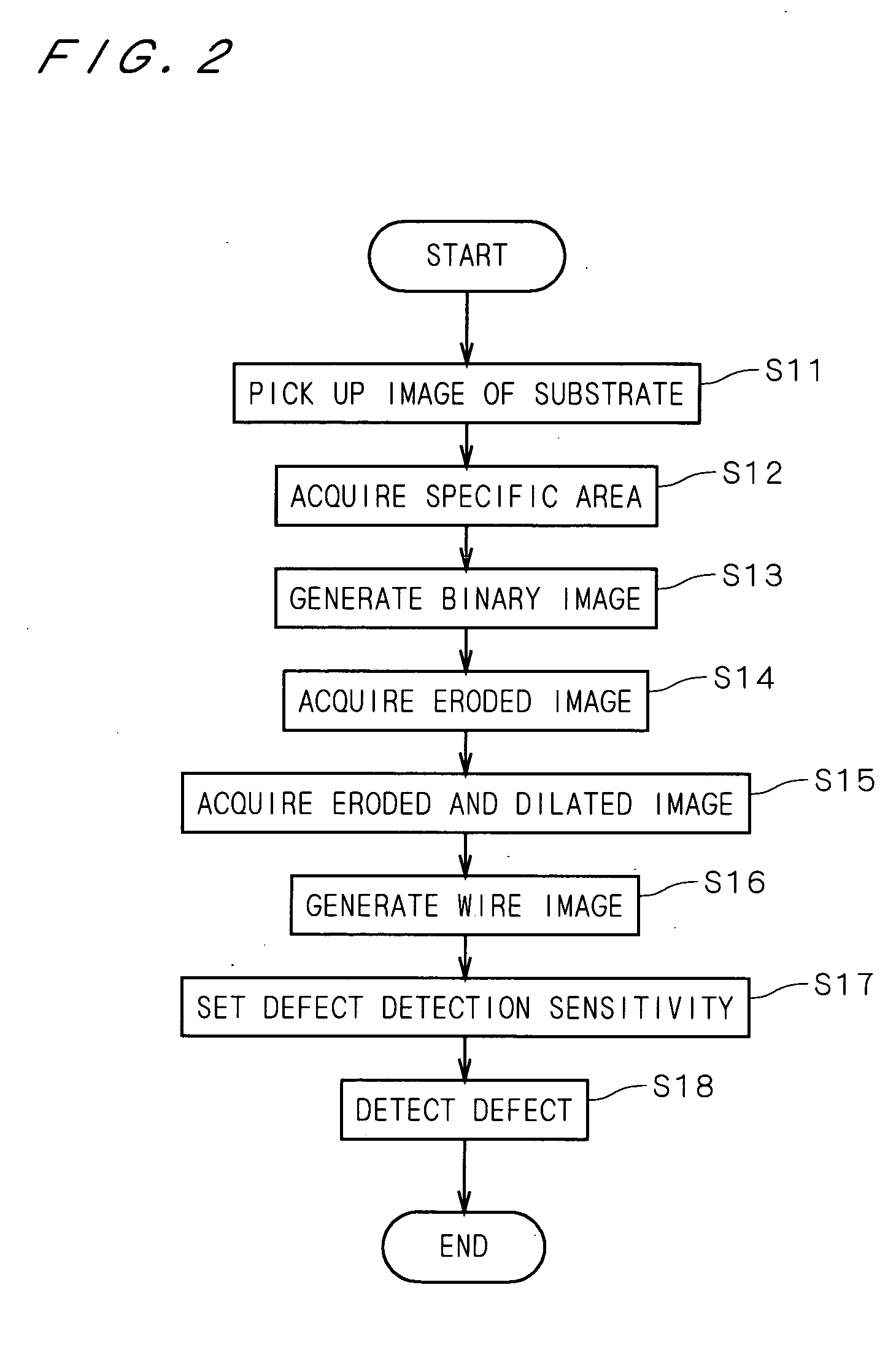
[0038]FIG. 1 is a view showing a construction of a defect detection apparatus 1 in accordance with the first preferred embodiment of the present invention. The defect detection apparatus 1 comprises a stage part 2 for holding a printed circuit board on which a pattern including wires (traces) is formed (hereinafter, referred to as “substrate”) 9, an image pickup part 3 for picking up an image of the substrate 9 to acquire a color image of the substrate 9 for inspection and a stage driving part 21 for moving the stage part 2 relatively to the image pickup part 3.
[0039] The stage part 2 has a transmitting illumination part 20 for emitting white light towards a lower main surface of the substrate 9 which is the opposite side of an upper surface facing the image pickup part 3. The image pickup part 3 has a lighting part 31 for emitting illumination light, an optical system 32 for guiding the illumination light to the substrate 9 and receiving light from the substrate 9 and an image pic...
PUM
| Property | Measurement | Unit |
|---|---|---|
| defect detection | aaaaa | aaaaa |
| area | aaaaa | aaaaa |
| defect detection sensitivities | aaaaa | aaaaa |
Abstract
Description
Claims
Application Information