Method for manufacturing semiconductor device

a manufacturing method and semiconductor technology, applied in the direction of semiconductor devices, basic electric elements, electrical appliances, etc., can solve the problems of increasing the on-resistance, unable to obtain unable to achieve the desired threshold voltage vsub>gsoff/sub>, so as to improve the characteristics and stability of the element, reduce the on-resistance, and prevent the effect of diffusion caused by heat treatmen

Active Publication Date: 2005-11-17
SEMICON COMPONENTS IND LLC
View PDF12 Cites 14 Cited by
  • Summary
  • Abstract
  • Description
  • Claims
  • Application Information

AI Technical Summary

Benefits of technology

[0030] Specifically, charges generated on the surface of the substrate by diffusion of hydrogen can be removed. Thus, improvement and stability in characteristics of an element can be realized. To be more specific, in an insulating gate type semiconductor device, a desired threshold voltage VGSOFF can be obtained.
[0031] Therefore, for example, in an n-channel MOSFET, it is no longer required to increase an impurity concentration in a channel layer more than necessary in order to obtain a desired threshold voltage VGSOFF, which can contribute to a reduction in an on-resistance.
[0032] Moreover, by forming the opening of the barrier metal layer in a part of the insulating film, the element region is covered with the barrier metal layer, and an Al layer that is the wiring layer and the silicon substrate do not come into contact with each other. Therefore, diffusion caused by heat treatment after formation of the wiring layer can be prevented, and deposition of silicon nodules can be suppressed.
[0033] Particularly, in a MOSFET having a trench structure, an opening is also provided on the interlayer insulating film, and the source region and the body region are covered with the barrier metal layer. Specifically, the Al layer that is the wiring layer and the silicon substrate do not come into contact with each other. Thus, deposition of the silicon nodules can be suppressed. Therefore, a contact region between the body region, that is a minute region, and the wiring layer is not blocked, and a potential of the substrate is stabilized.
[0034] Second, the opening can be formed only by adding a step of etching a part of the barrier metal layer on the insulating film. Thus, sufficient hydrogen can be allowed to reach the substrate. Since diffusion of hydrogen proceeds isotropically from the opening, sufficient hydrogen passing through the opening can be allowed to reach the substrate. Therefore, under hydrogen annealing conditions similar to those of the conventional case, an amount of hydrogen which reaches the substrate can be increased.
[0035] Particularly, in the MOSFET having the trench structure, the opening of the barrier metal layer can be formed by use of a mask for trench formation. Specifically, an opening can be provided only on the interlayer insulating film without newly creating a mask for the opening. Therefore, it is possible to provide a method of manufacturing a semiconductor device, which prevents an increase in the number of masks, and obtains a desired threshold voltage VGSOFF.

Problems solved by technology

However, because of a high diffusion rate of Si in Al, Al and Si are diffused to cause a phenomenon called a spike which destroys a pn junction.
Moreover, since the Si nodule itself has a high resistance, the Si nodule becomes a factor that causes an unstable contact resistance or increases a contact resistance.
However, depending on a kind of a barrier, a desired threshold voltage VGSOFF may not be obtained even if heat treatment in a hydrogen-containing gas atmosphere (hereinafter referred to as hydrogen annealing) is performed.
Thus, there is a problem that an on-resistance is increased.
Specifically, in the conventional method, there is a problem that a substantial effect of hydrogen annealing treatment for removing charges of the substrate is not obtained due to the barrier metal layer which prevents the spike and avoids the contact failure caused by the Si nodule.

Method used


Image

  • Method for manufacturing semiconductor device
  • Method for manufacturing semiconductor device
  • Method for manufacturing semiconductor device

Examples


Embodiment Construction

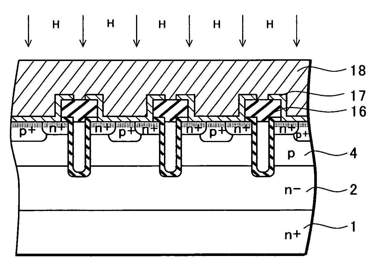
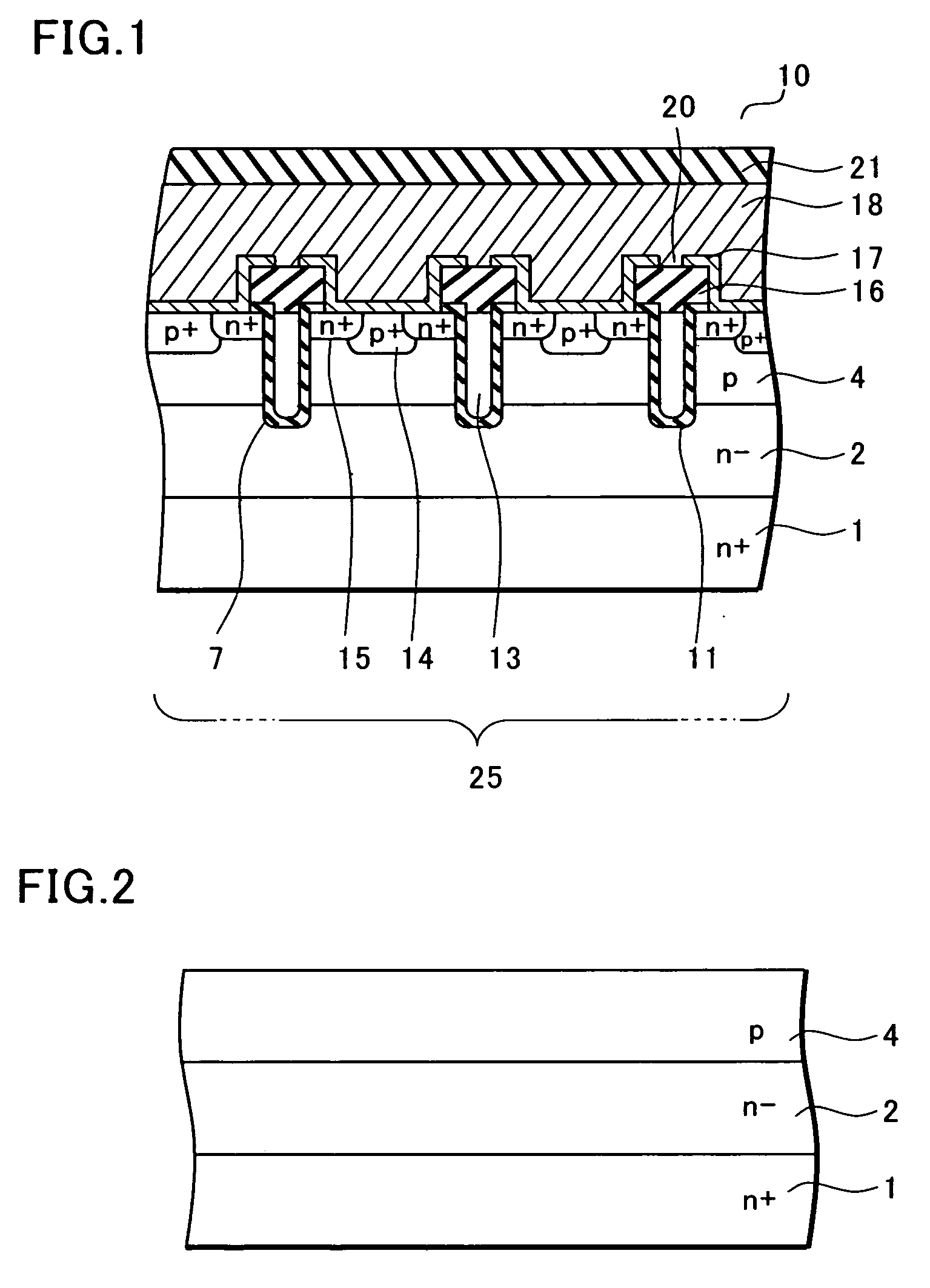
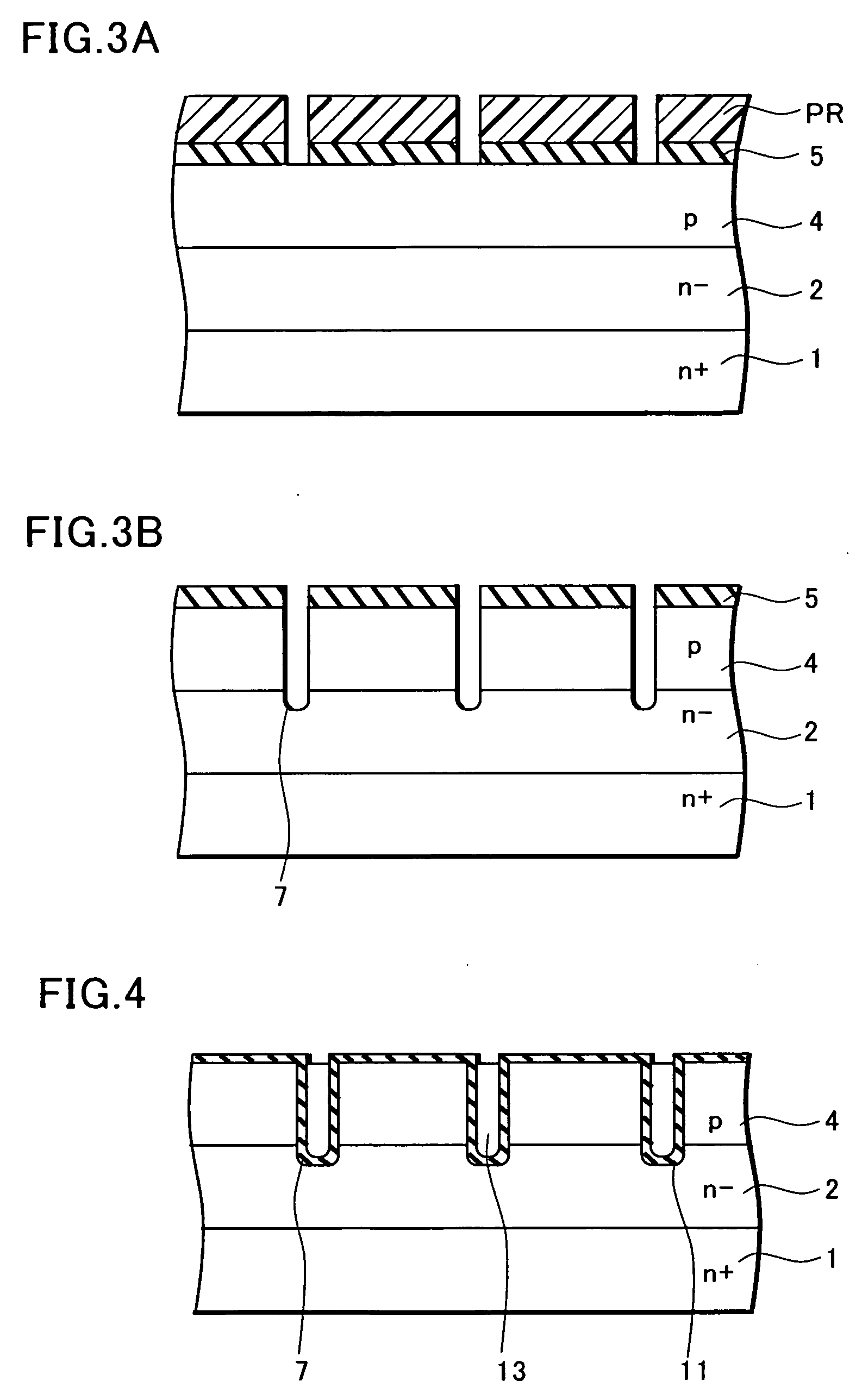
[0049] With reference to FIGS. 1 to 10B, detailed description will be given of an embodiment of the present invention by taking an n-channel MOSFET having a trench structure as an example.

[0050]FIG. 1 is a cross-sectional view showing a structure of a MOSFET 10 of the present invention. The MOSFET 10 includes a silicon semiconductor substrate 1, a semiconductor layer 2, a channel layer 4, a trench 7, an insulating film 11, a gate electrode 13, a source region 15, a body region 14, an interlayer insulating film 16, a first metal layer 17, an opening 20, and a second metal layer 18.

[0051] A drain region is formed by laminating an n− type epitaxial layer 2 on the n+ type silicon semiconductor substrate 1, and the like.

[0052] The channel layer 4 is a region obtained by diffusing p-type impurities on a surface of the n− type semiconductor layer 2. The trench 7 is provided so as to penetrate the channel layer 4 and to have a depth reaching the drain region 2. An inner wall of the trenc...


PUM

PropertyMeasurementUnit
temperatureaaaaaaaaaa
thicknessaaaaaaaaaa
thicknessaaaaaaaaaa

Abstract

In a MOSFET, after an element region is formed, a wiring layer is formed subsequently to a barrier metal layer, and hydrogen annealing is performed. However, in the case of an n-channel MOSFET, a threshold voltage is lowered due to an occlusion characteristic of the barrier metal layer. Thus, an increased impurity concentration in a channel layer causes a problem that reduction in an on-resistance is inhibited. According to the present invention, after a barrier metal layer is formed, an opening is provided in the barrier metal layer on an interlayer insulating film, and hydrogen annealing treatment is performed after a wiring layer is formed. Thus, an amount of hydrogen which reaches a substrate is further increased, and lowering of a threshold voltage is suppressed. Moreover, since an impurity concentration in a channel layer can be lowered, an on-resistance is reduced.

Description

BACKGROUND OF THE INVENTION [0001] 1. Field of the Invention [0002] The present invention relates to a method of manufacturing a semiconductor device, and more particularly relates to a method of manufacturing a semiconductor device, which improves characteristics by allowing sufficient hydrogen to reach a substrate surface in hydrogen annealing treatment. [0003] 2. Description of the Related Art [0004] With reference to FIGS. 11 to 13, description will be given of a conventional semiconductor device by taking an n-channel MOSFET having a trench structure as an example. [0005] First, FIG. 11 shows a structure of a MOSFET 40. An n− type epitaxial layer 22 is laminated on an n+ type silicon semiconductor substrate 21 to provide a drain region, and a p-type channel layer 24 is provided thereon. [0006] Trenches 27 are provided, which penetrate the channel layer 24 and reach the drain region 22. Inner walls of the trenches 27 are covered with a gate oxide film 31, and the trenches 27 are...

Claims


Application Information

Patent Timeline
Patent Type & Authority Applications(United States)
IPC IPC(8): H01L21/30H01L21/31H01L21/322H01L21/336H01L21/28H01L21/469H01L21/768H01L21/8234H01L27/10H01L29/417H01L29/45H01L29/74H01L29/78
CPCH01L21/3003H01L21/76886H01L29/7813H01L29/456H01L21/823487H01L29/66734
Inventor ISHIDA, HIROYASUKUBO, HIROTOSHIMIYAHARA, SHOUJIONDA, MASATO
Owner SEMICON COMPONENTS IND LLC
Why Eureka
Try Eureka