Process for producing electrical apparatus
a technology of electrical equipment and process, applied in the direction of chemistry apparatus and processes, adhesive processes with surface pretreatment, printed circuit aspects, etc., can solve the problems of reducing the life of adhesives, affecting the efficiency of adhesives, and affecting the quality of adhesives
- Summary
- Abstract
- Description
- Claims
- Application Information
AI Technical Summary
Benefits of technology
Problems solved by technology
Method used
Image
Examples
example 1
[0057] First, an Example 1 of the method for producing an electrical device according to the present invention is explained.
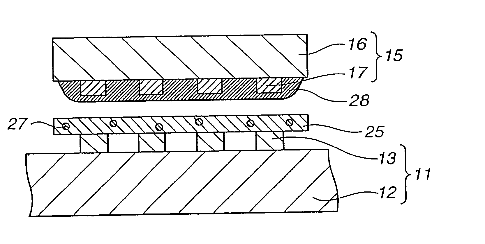
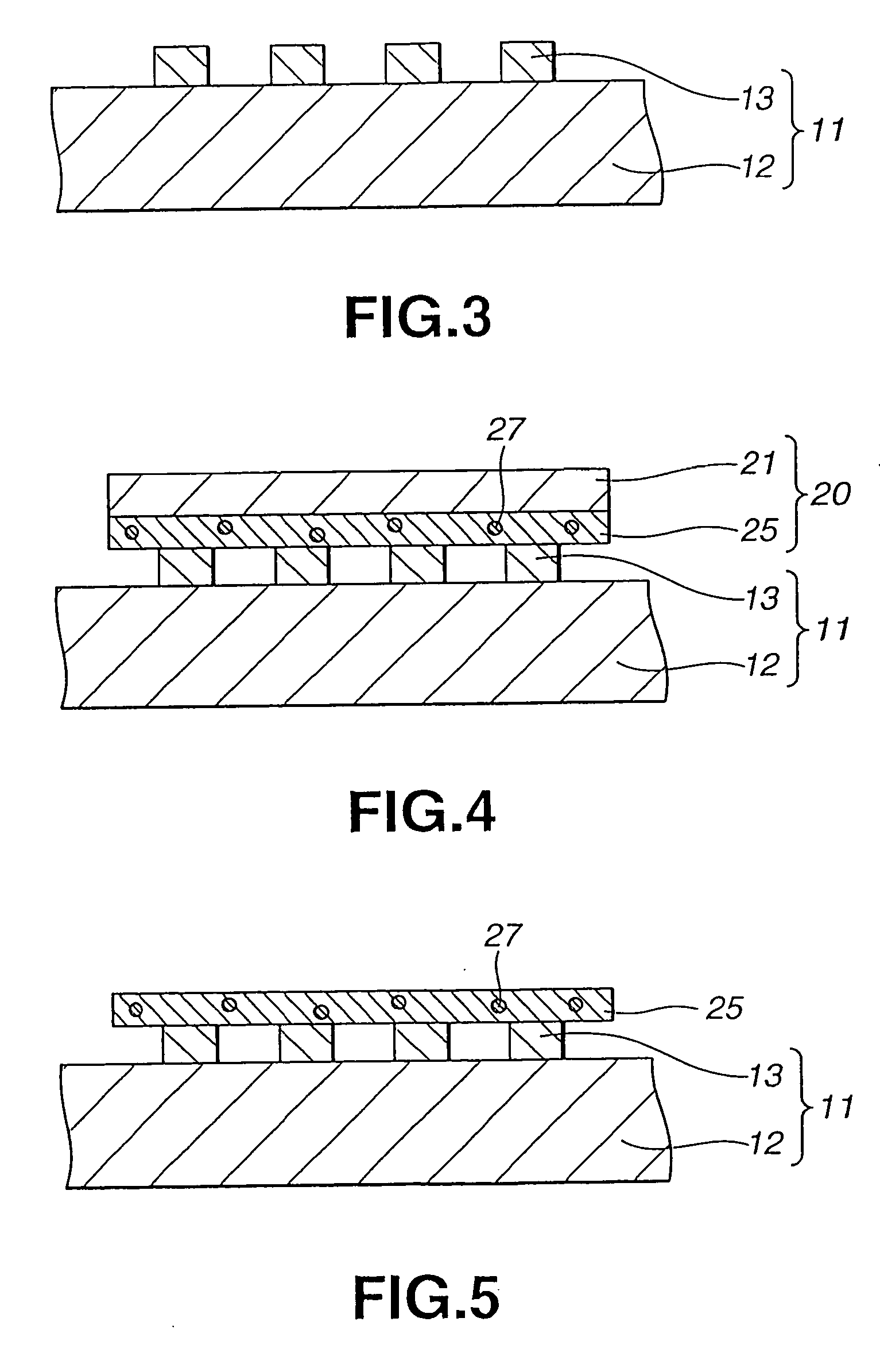
[0058] In the present Example 1, the LCD 11 and the TCP 15 are bonded together, using an adhesive, as now explained, to produce an electrical device.
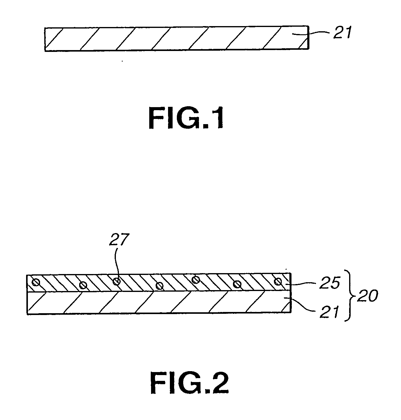
[0059] A paste-like adhesive was prepared by mixing 5 parts by weight of an epoxy silane coupling agent (manufactured by SHIN-ETSU KAGAKU KOGYO KK under a trade name of ‘KBM-403’), as a first curing agent, 40 parts by weight of alicyclic epoxy resin celoxide (manufactured and sold by DICEL KAGAKU KOGYO KK under the trade name of ‘2021P’) as an epoxy resin, 60 parts by weight of bisphenol A epoxy resin as an epoxy resin (manufactured and sold by YUKA SHELL EPOXY KK under the trade name of ‘EP1009’) and10 parts by weight of electrically conductive particles. This adhesive was coated to a film thickness of 20 μm on the surface of the release film 21 to form the adhesive layer 25 to produce the adhesive film 20. The ...
example 2
[0063] In the Example 1, the adhesive layer 25 was prepared in the same way as in Example 1, except using the metal chelate, used in Example 1, in place of the epoxy silane coupling agent, as the first curing agent.
[0064] Moreover, the epoxy silane coupling agent, used in Example 1, was provided as the second curing agent, in place of the metal chelate.
[0065] In this Example 2, the adhesive film 20 used was again an adhesive coated on the release film 21 to form the adhesive layer 25.
[0066] The LCD 11, carrying the adhesive layer 25, and the TCP 15, carrying the layer of the second curing agent 28, formed by the second curing agent, are bonded together through a process similar to the process of the above Example 1 to give the electrical device 10 of Example 2.
example 3
[0067] In the Example 3, the following adhesive was used. For producing the adhesive, 50 parts by weight of a product (manufactured and sold by DICEL KAGAKU KOGYO KK under the trade name of celoxide ‘2021P’) as an epoxy resin, and 50 parts by weight of a product (manufactured and sold by YUKA SHELL EPOXY KK under the trade name of ‘EP100’) as an epoxy resin, were mixed together. The resulting mixture was stirred, as it was kept at 70° C., to form a solution of paste-like epoxy resin. To 100 parts by weight of this solution of paste-like epoxy resin, 5 parts by weight of the first curing agent (epoxy silane coupling agent) used in Example 1 and 10 parts by weight of the electrically conductive particles, used in Example 1, were added and mixed together to form a paste-like adhesive. The adhesive, thus prepared, is coated on the surface of the LCD 11 of Example 1, carrying the first electrodes 13, to form an adhesive layer 75.
[0068] On the other hand, the layer of the second curing a...
PUM
| Property | Measurement | Unit |
|---|---|---|
| Temperature | aaaaa | aaaaa |
| Electrical conductivity | aaaaa | aaaaa |
Abstract
Description
Claims
Application Information


