Light emitting device

a light emitting device and active matrix technology, applied in the direction of solid-state devices, electric lighting sources, electric light sources, etc., can solve the problems of deterioration of image visibility

Inactive Publication Date: 2005-11-24
SEMICON ENERGY LAB CO LTD
View PDF16 Cites 26 Cited by
  • Summary
  • Abstract
  • Description
  • Claims
  • Application Information

AI Technical Summary

Benefits of technology

[0012] By applying the structure of the light emitting device according to the invention, it is possible to provide a light emitting device in which the variation in emission spectrum depending on an angle for seeing a surface through which light is emitted is reduced.

Problems solved by technology

This causes problems in which the emission spectrum is changed depending on an angle for seeing a surface through which light is emitted, and the visibility of an image displayed on the light emitting device is deteriorated.
Also, the deterioration in visibility of an image, which is caused due to the variation in refractive index for each layer, is also caused in a passive matrix light emitting device.
For example, the patent document 1 raises a problem in which the visibility is deteriorated by reflecting outside light and light emitted from a light emitting element at an interface due to the variation in refractive index of respective layers constituting the light emitting element.

Method used


Image

  • Light emitting device
  • Light emitting device
  • Light emitting device

Examples


embodiment mode 1

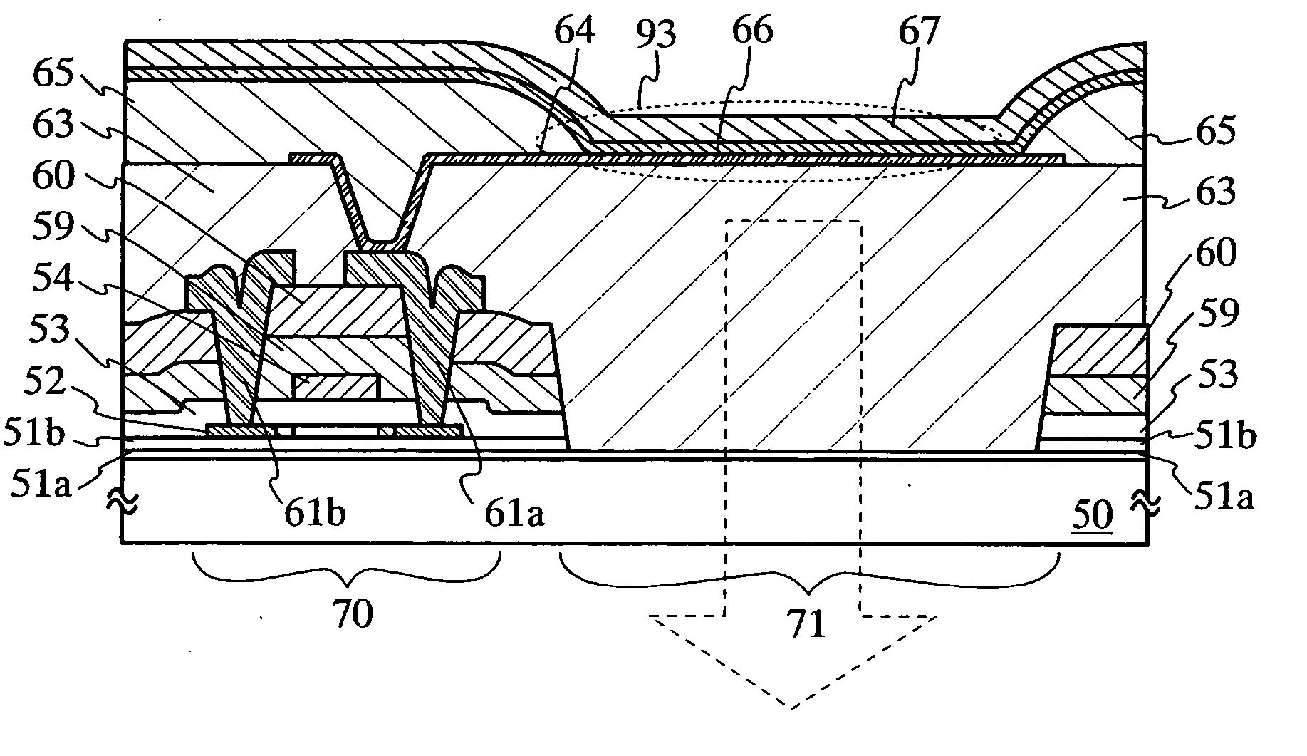
[0030] A light emitting device of the present invention will be described with reference to FIG. 1. A first base insulating layer 51a and a second base insulating layer 51b are provided over a substrate 50. A thin film transistor 70 including a semiconductor layer 52, a gate insulating layer 53 and a gate electrode 54 is formed on the second base insulating layer 51b. Also, the thin film transistor 70 is covered with an insulating film (a hydrogenated film) 59 and a first interlayer insulating layer 60. A connection portion (wiring) 61a and a wiring 61b that also serve as a source electrode and a drain electrode of the thin film transistor 70 are formed on the first interlayer insulating layer 60. The connection portion 61a and the wiring 61b are partly and electrically connected to the semiconductor layer 52 through contact holes passing through the insulating film (hydrogenated film) 59, the first interlayer insulating layer 60 and the gate insulating layer 53. A second interlayer...

embodiment mode 2

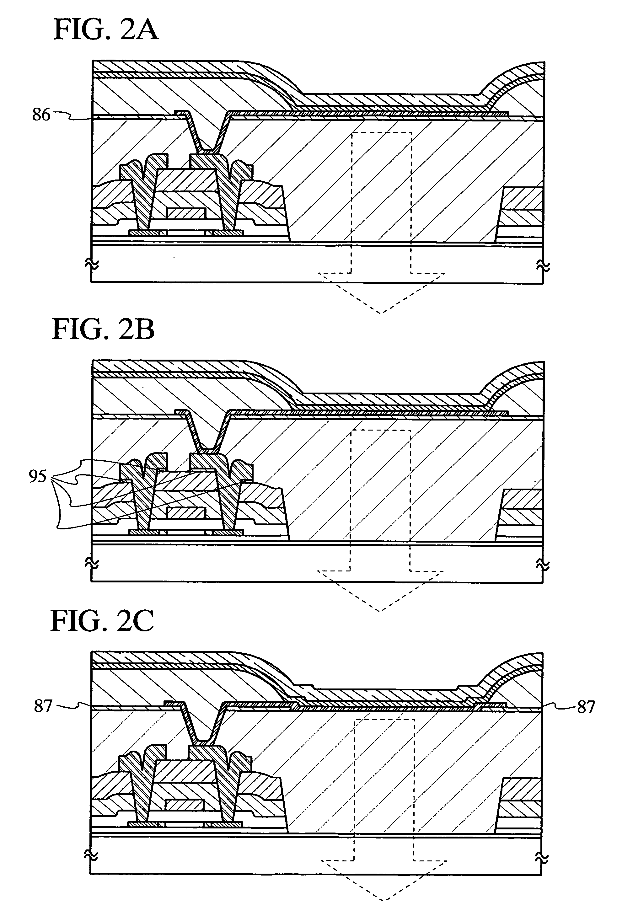
[0053] In this embodiment mode, another structures of the invention will be shown in FIGS. 2A to 2C. The structures described in this embodiment mode exhibit same effect as that of the structure described in Embodiment Mode 1. Characteristics of the respective structures will be described below. Further, portions identical to those of FIG. 1 are not denoted by the reference numerals, and will not be further explained. Refer to FIG. 1 and Embodiment Mode 1 for more information about the portions.

[0054] As shown in FIG. 2A, an insulating layer 86 made from a material different from that of the second interlayer insulating layer 63 may be formed on the second interlayer insulating layer 63. The insulating layer 86 is made from a silicon nitride film or the like. This insulating layer 86 serves to prevent the second interlayer insulating layer 63 from being etched in etching the first electrode 64 of the light emitting element 93 and serves to prevent ingress of moisture etc., which ad...

embodiment mode 3

[0059] Another embodiment mode of the invention will be described in FIGS. 3A to 3C. The structures as shown in the present embodiment mode exhibit same effect as that of Embodiment Mode 1. Characteristics of the respective structures will be described below. Further, portions identical to those of FIG. 1 are not denoted by the reference numerals and will not be further explained. Refer to FIG. 1 and Embodiment Mode 1 for more information about the portions.

[0060]FIGS. 3A to 3C show cases where insulating layers 80, 82 and 84 are formed on each connection portion 61a and each wiring 61b. These insulating layers are used as passivation films for preventing active layers of the thin film transistors from an impurity. Therefore, a film mainly containing silicon nitride with an excellent passivation property is used as these insulating films. However, they may be formed of other material.

[0061] When forming the insulating layer 80, 82 or 84, if a refractive index of the insulating lay...


PUM


Abstract

An object of the invention is to provide a light emitting device in which the variation in emission spectrum depending on an angle for seeing a surface through which light is emitted is reduced. The light emitting device of the invention includes a first insulating layer formed over a substrate, a second insulating layer formed over the first insulating layer, and a semiconductor layer formed over the second insulating layer. A gate insulating layer is formed to cover the second insulating layer and the semiconductor layer. A gate electrode is formed over the gate insulating layer. A first interlayer insulating layer is formed to cover the gate insulating layer and the gate electrode. An opening is formed through the first interlayer insulating layer, the gate insulating layer and the second insulating layer. A second interlayer insulating layer is formed to cover the first insulating layer and the opening. A light emitting element is formed over the opening.

Description

BACKGROUND OF THE INVENTION [0001] 1. Field of the Invention [0002] The present invention relates to an active matrix light emitting device, and in particular, relates to a structure of a portion through which light is emitted. [0003] 2. Description of the Related Art [0004] A light emitting device utilizing light emitted by an electroluminescent element (a light emitting element) has been attracting attention as a display device with a wide viewing angle and low power consumption. [0005] Light emitting devices that are mainly used for displaying images are classified into an active matrix light emitting device and a passive matrix light emitting device. An active matrix light emitting device can control lighting, non-lighting and the like of light emitting elements for each light emitting element. Therefore, the active matrix light emitting device can be driven at lower power consumption than a passive matrix light emitting device, and hence, the active matrix display device is sui...

Claims


Application Information

Patent Timeline
Patent Type & Authority Applications(United States)
IPC IPC(8): H01L27/15H01L27/32H01L33/00H05B33/12H05B44/00
CPCH01L27/3244H01L51/5262H01L27/3258H01L27/3248H10K59/123H10K59/12H10K59/124H10K50/85
Inventor YAMAZAKI, SHUNPEIOHNUMA, HIDETOANZAI, AYASAKAKURA, MASAYUKIGODO, HIROMICHI
Owner SEMICON ENERGY LAB CO LTD
Why Eureka
Try Eureka