

Semiconductor device mounting structure
- Summary
- Abstract
- Description
- Claims
- Application Information
AI Technical Summary
Benefits of technology
Problems solved by technology
Method used
Image

Examples
first embodiment
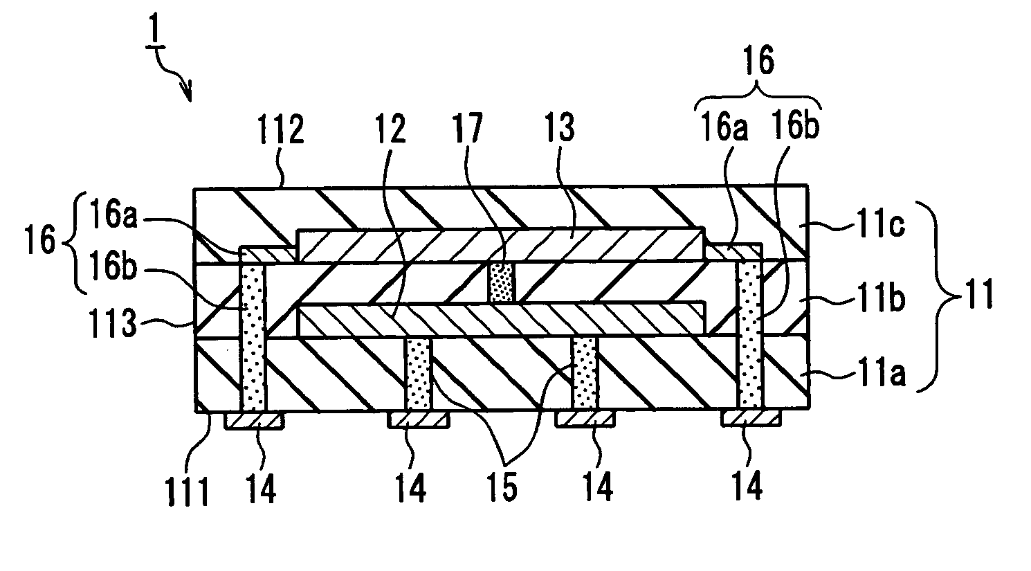
[0032] Firstly, a first embodiment of the present invention will be described with reference to the accompanying drawings as appropriate. FIG. 1 referenced here is a schematic cross-sectional view of a semiconductor device mounting structure according to a first embodiment of the present invention.
[0033] As shown in FIG. 1, a semiconductor device mounting structure 1 according to the first embodiment includes: an electrically insulating layer 11 that includes electrically insulating substrates 11a, 11b, and 11c; a first semiconductor device 12 arranged in the electrically insulating layer 11b; a second semiconductor device 13 arranged in the electrically insulating layer 11c; heat dispersion portions 14 provided on a main surface 111 on the electrically insulating layer 11a side of the electrically insulating layer 11; first heat-conducting paths 15 connected to the heat dispersion portions 14 and the first semiconductor device 12; second heat-conducting paths 16 connecting the hea...
second embodiment
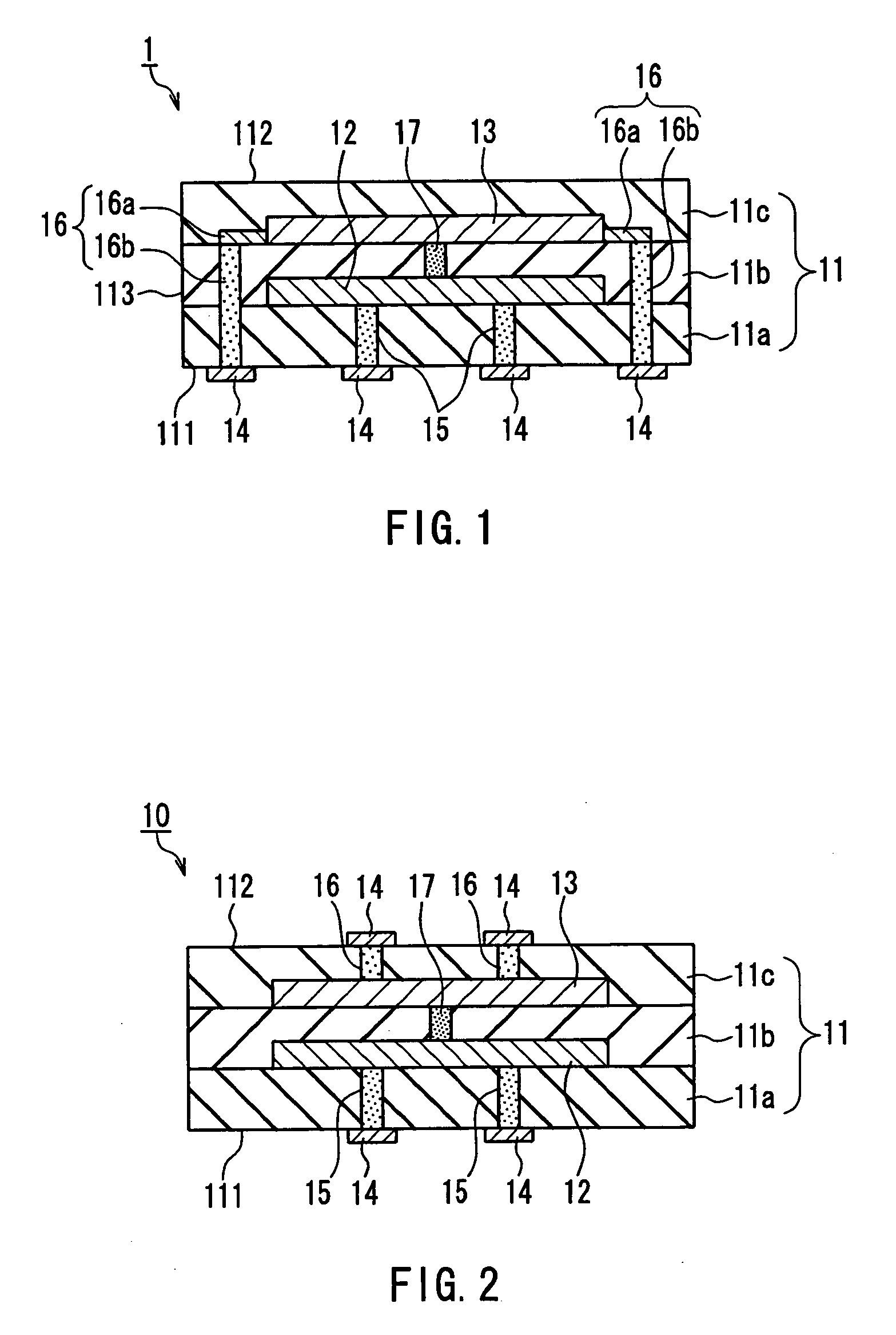
[0036] Next, a second embodiment of the present invention will be described with reference to the accompanying drawings as appropriate. FIG. 3 referenced here is a schematic cross-sectional view of a semiconductor device mounting structure according to a second embodiment of the present invention. It should be noted that in FIG. 3, members having the same structure as the semiconductor device mounting structure 1 according to the above-described first embodiment (see FIG. 1) will be given the same numerical symbol and the description thereof will be omitted.
[0037] As shown in FIG. 3, a semiconductor device mounting structure 2 according to the second embodiment includes an electrically insulating layer 21 that includes four layers of electrically insulating substrates 21a to 21d, and a shared heat-conducting path 22 provided in the electrically insulating substrate 21b, with the first and second heat-conducting paths 15 and 16 being connected to the shared heat-conducting path 22. ...
third embodiment
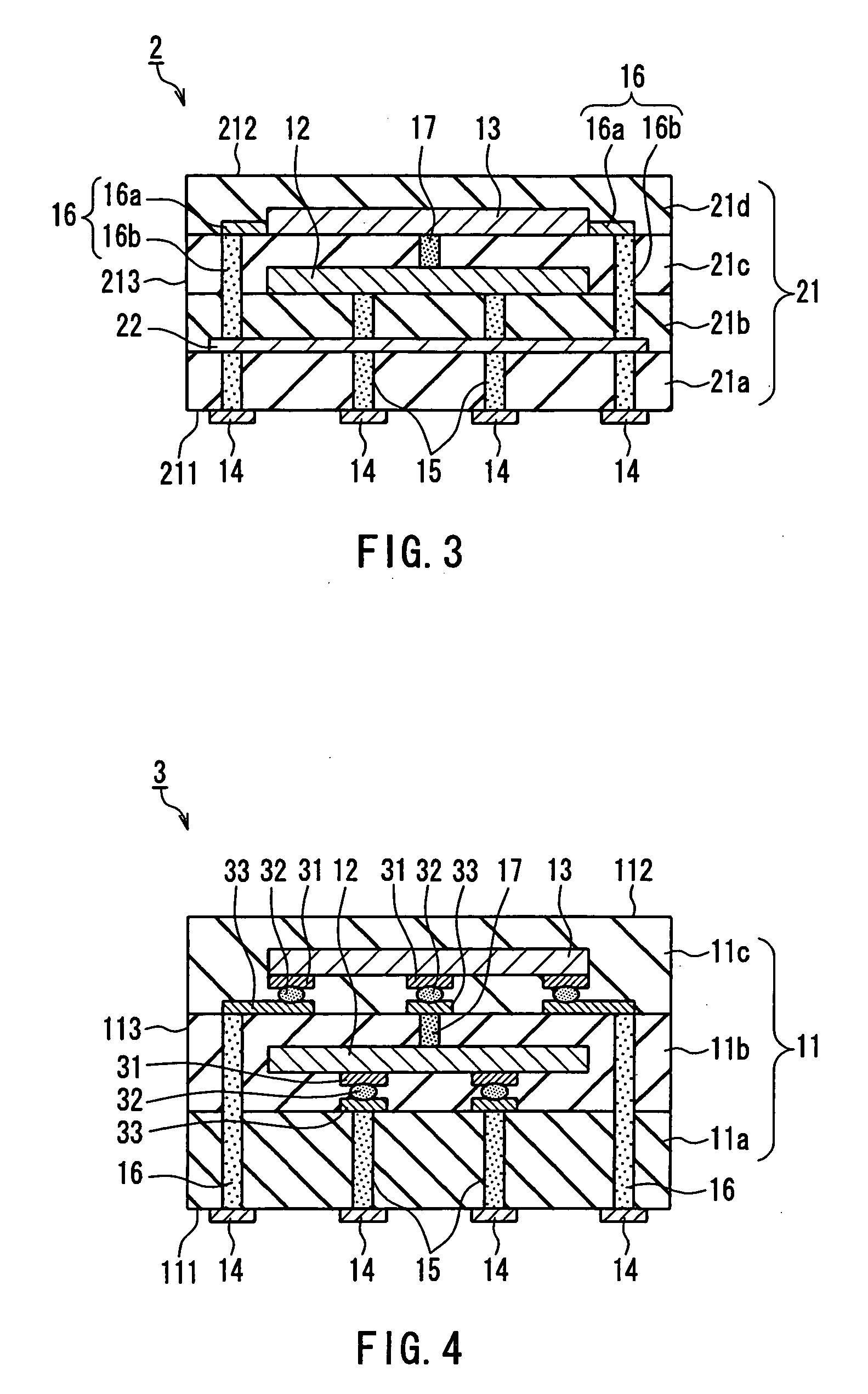
[0039] Next, a third embodiment of the present invention will be described with reference to the accompanying drawings as appropriate. FIG. 4 referenced here is a schematic cross-sectional view of a semiconductor device mounting structure according to a third embodiment of the present invention. It should be noted that in FIG. 4, members having the same structure as the semiconductor device mounting structure 1 according to the above-described first embodiment (see FIG. 1) will be given the same numerical symbol and description thereof will be omitted.
[0040] As shown in FIG. 4, in a semiconductor device mounting structure 3 according to the third embodiment, the first and second semiconductor devices 12 and 13 are flip chip mounted. Furthermore, the second heat-conducting paths 16 are constituted by thermal vias formed in the thickness direction of the electrically insulating substrates 11a and 11b. Furthermore, in locations where the first semiconductor device 12 and the first hea...
PUM
 Abstract
Description
Claims
Application Information