High-speed interface circuit test module, module under high-speed interface circuit test, and high-speed interface circuit test method

a high-speed interface and test module technology, applied in the direction of individual semiconductor device testing, data switching networks, instruments, etc., can solve the problems of increased test cost, insufficient characteristic assurance, and increased cost of high-speed lsi testers, so as to ensure test quality and maintainability.

Inactive Publication Date: 2005-11-24
PANASONIC CORP
View PDF7 Cites 34 Cited by
  • Summary
  • Abstract
  • Description
  • Claims
  • Application Information

AI Technical Summary

Benefits of technology

[0010] The present invention is made in view of the above-mentioned problem, and an object thereof is to provide a high-speed interface circuit test module, a module under high-speed interface circuit inspection and a high-speed interface circuit test method capable of guaranteeing the communication characteristics at low test cost and efficiently performing the debugging of the high-speed transmission line on the board by solving the problem that in the shipment test of LSIs provided with a high-speed interface circuit, it is impossible to realize both cost reduction and a high test guarantee level because the test is realized by using a high-speed LSI tester that leads to an increase in test cost or providing a high-speed interface circuit having fixed transmission and reception characteristics on the DUT board.

Problems solved by technology

High-speed LSI testers are generally more expensive than low-speed LSI testers.
Consequently, the cost of the test is increased.
In the latter case, although the increase in the cost of the test can be suppressed, since the characteristic test of the high-speed interface circuit cannot be performed, there is a possibility that the guarantee of the characteristics is insufficient, so that there is a possibility that defectives flow out.
Moreover, generally, it is impossible to possess, for boards and test program debugging, a multiplicity of LSI testers which are expensive equipment.
Therefore, it is extremely inefficient to use an LSI tester for debugging of the high-speed transmission line on the DUT board.

Method used


Image

  • High-speed interface circuit test module, module under high-speed interface circuit test, and high-speed interface circuit test method
  • High-speed interface circuit test module, module under high-speed interface circuit test, and high-speed interface circuit test method
  • High-speed interface circuit test module, module under high-speed interface circuit test, and high-speed interface circuit test method

Examples


first embodiment

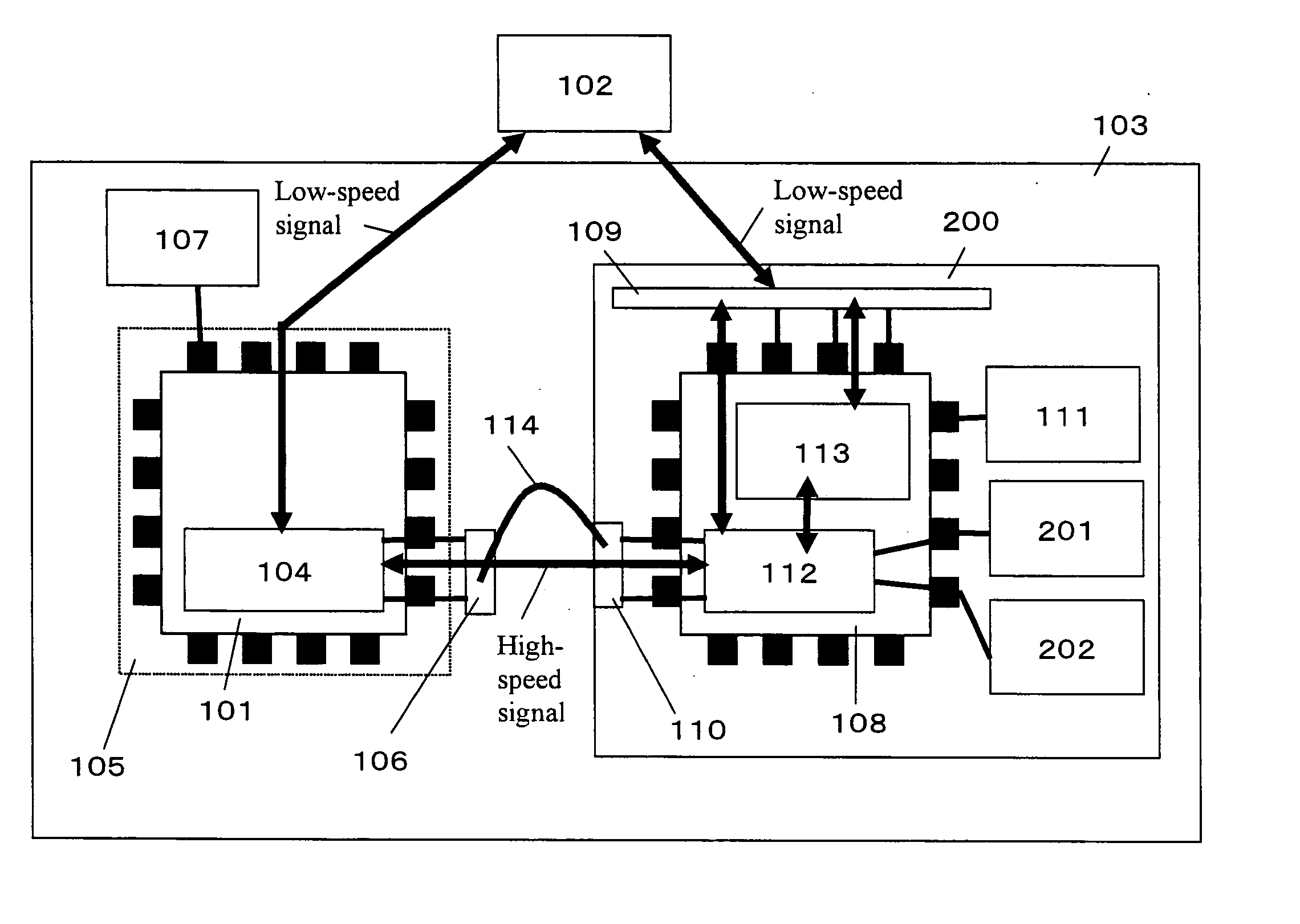
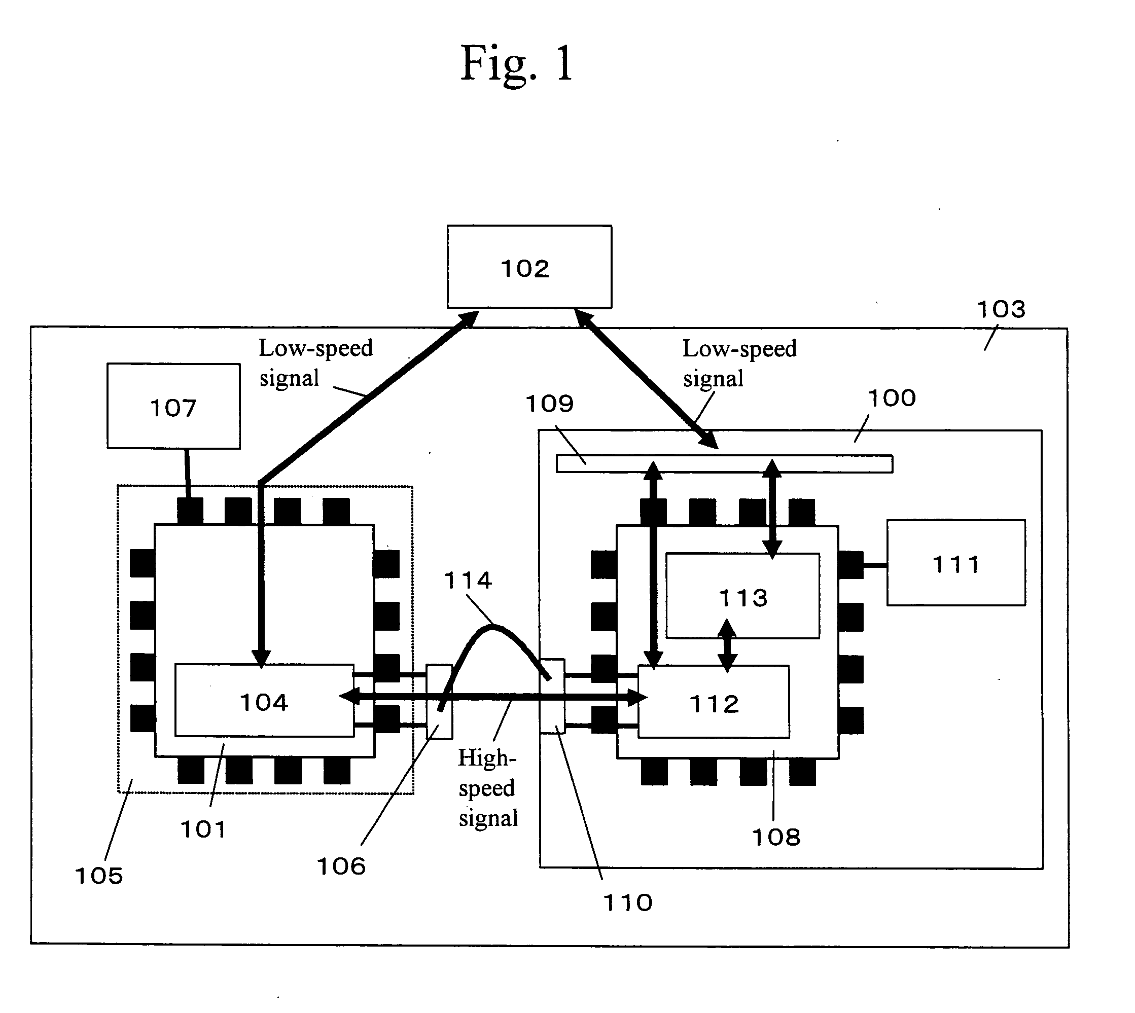
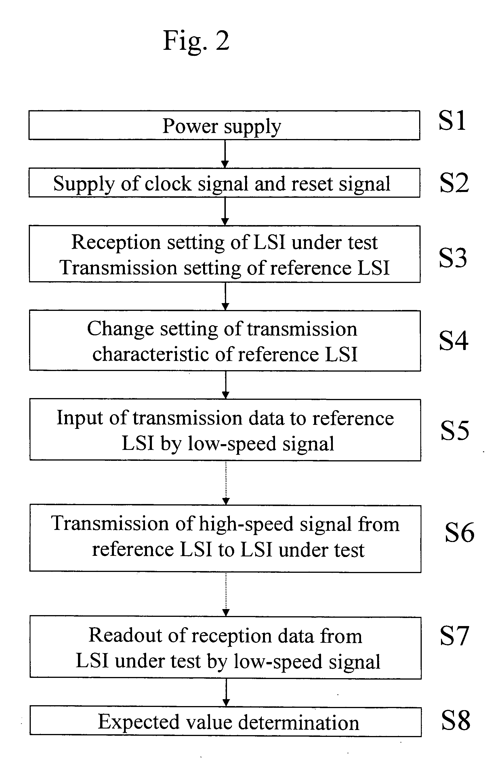
[0084] First, a reception test of the high-speed interface circuit 104 of the LSI under test 101 will be described. FIG. 2 is the control flow of the test according to the present invention.

[0085] A predetermined test voltage is supplied from the LSI tester 102 to the power terminals and the input terminals of the LSI under test 101 and the reference LSI 108 (S1), and a reset signal is supplied. Moreover, the clock signal is supplied to the LSI under test 101 and the reference LSI 108 by the clock generator 107 and the clock generator 111 (S2). The clock signal may be supplied from the LSI tester 102 by way of the load board 103 and the second connector 109 for low-speed signal communication (the method by the structure according to claim 6). Then, the high-speed interface circuit 104 of the LSI under test 101 and the high-speed interface circuit 112 of the reference LSI 108 on the high-speed interface circuit test module 100 are accessed from the LSI tester 102 by the low-speed sig...

third embodiment

[0126] A third embodiment of the present invention will be described with reference to FIG. 7. As the third embodiment, an embodiment according to claims 8, 9 and 10 will be described. FIG. 7 shows the structure of an LSI test using a high-speed interface circuit test module 300 according to the present invention. Circuits having the same functions as those of the first embodiment are denoted by the same reference numerals.

[0127] The structure of this embodiment is different from that of the first embodiment in that a frequency modulator 301 or a jitter injector 302 is newly provided on the high-speed interface circuit test module 300 so as to adjoin the clock generator 111.

[0128] The frequency modulator 301 is connected to the output terminal of the clock generator 111 and to the clock input terminal of the reference LSI 108, and supplies a spectrum modulation clock signal. The spectrum modulation clock is a clock whose clock frequency changes at predetermined intervals. The clock...


PUM


Abstract

In the shipment test of an LSI provided with a high-speed interface circuit, both cost reduction and a high test guarantee level are realized. The following are provided: a high-speed interface circuit that is mounted on a load board interfacing with an LSI tester, is provided with a circuit converting the signal speed, and is capable of changing the transmission and reception characteristics; a controller that controls the transmission and reception characteristics of the high-speed interface circuit; a clock generator that generates the clock supplied to the high-speed interface circuit; a first connector provided specifically for the high-speed interface, connected to the high-speed interface circuit and provided with a signal port for performing high-speed signal communication with a circuit under test; and a second connector connected to the high-speed interface circuit and the LSI tester and provided with a signal port and a power port for performing low-speed signal communication with the high-speed interface circuit.

Description

BACKGROUND OF THE INVENTION [0001] 1. Field of the Invention [0002] The present invention relates to a high-speed interface circuit test module being a test module for an LSI provided with a high-speed interface circuit, a module under high-speed interface circuit test, and a high-speed interface circuit test method. [0003] 2. Description of the Prior Art [0004] Conventionally, a test of an LSI provided with a high-speed interface circuit such as IEEE 1394 or Serial ATA has been realized by use of a high-speed LSI tester capable of inputting and outputting high-speed signals (for example, see Non-patent Document 1). Moreover, there is a method that realizes the test without the use of a high-speed LSI tester by providing a high-speed interface circuit on a DUT (device under test) board (also called load board) (for example, see Hiroshi Kaga, “LSI tesuto kuraisisu no “keikou to taisaku” (“Tendency and Countermeasure” of LSI Test Crisis)”, Design Wave Magazine 2004 February, and Japan...

Claims


Application Information

Patent Timeline
Patent Type & Authority Applications(United States)
IPC IPC(8): G01R31/26G01R31/28G01R31/30G01R31/317G01R31/319G06F13/00H04L12/26
CPCG01R31/3016G01R31/31712H04L43/50G01R31/31926H04L12/2697G01R31/31905
Inventor KISHIMOTO, SATOSHIKANEMITSU, TOMOHIKOMAEKAWA, MICHIO
Owner PANASONIC CORP
Why Eureka
Try Eureka