Adjustable shielding plate for adjusting an etching area of a semiconductor wafer and related apparatus and methods

a shielding plate and etching area technology, applied in the direction of instruments, fluid pressure measurement, coatings, etc., can solve the problems of high processing cost, difficult to adjust the etching area of the edge portion of the wafer, and difficult process control

Inactive Publication Date: 2005-12-01
SAMSUNG ELECTRONICS CO LTD
View PDF6 Cites 75 Cited by
  • Summary
  • Abstract
  • Description
  • Claims
  • Application Information

AI Technical Summary

Problems solved by technology

However, wet etching may result in difficulties in process controls and high processing costs because of the etchant(s) used and the relatively long operational time that may be needed to reduce or remove the byproducts.
However, it may be difficult to adjust the etching area of the edge portion of the wafer using the dry etching process described above.
However, the gas dispersion plate 30 may be difficult, costly and / or time consuming to change.

Method used


Image

  • Adjustable shielding plate for adjusting an etching area of a semiconductor wafer and related apparatus and methods
  • Adjustable shielding plate for adjusting an etching area of a semiconductor wafer and related apparatus and methods
  • Adjustable shielding plate for adjusting an etching area of a semiconductor wafer and related apparatus and methods

Examples


Embodiment Construction

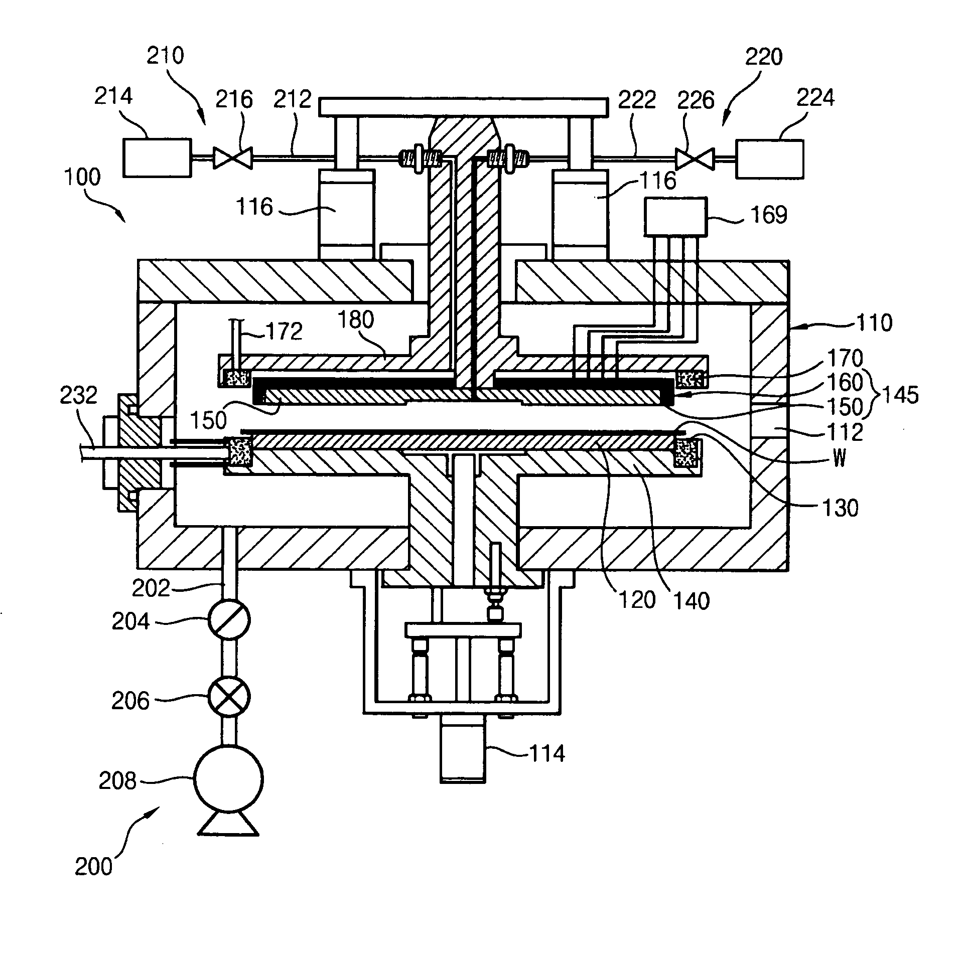
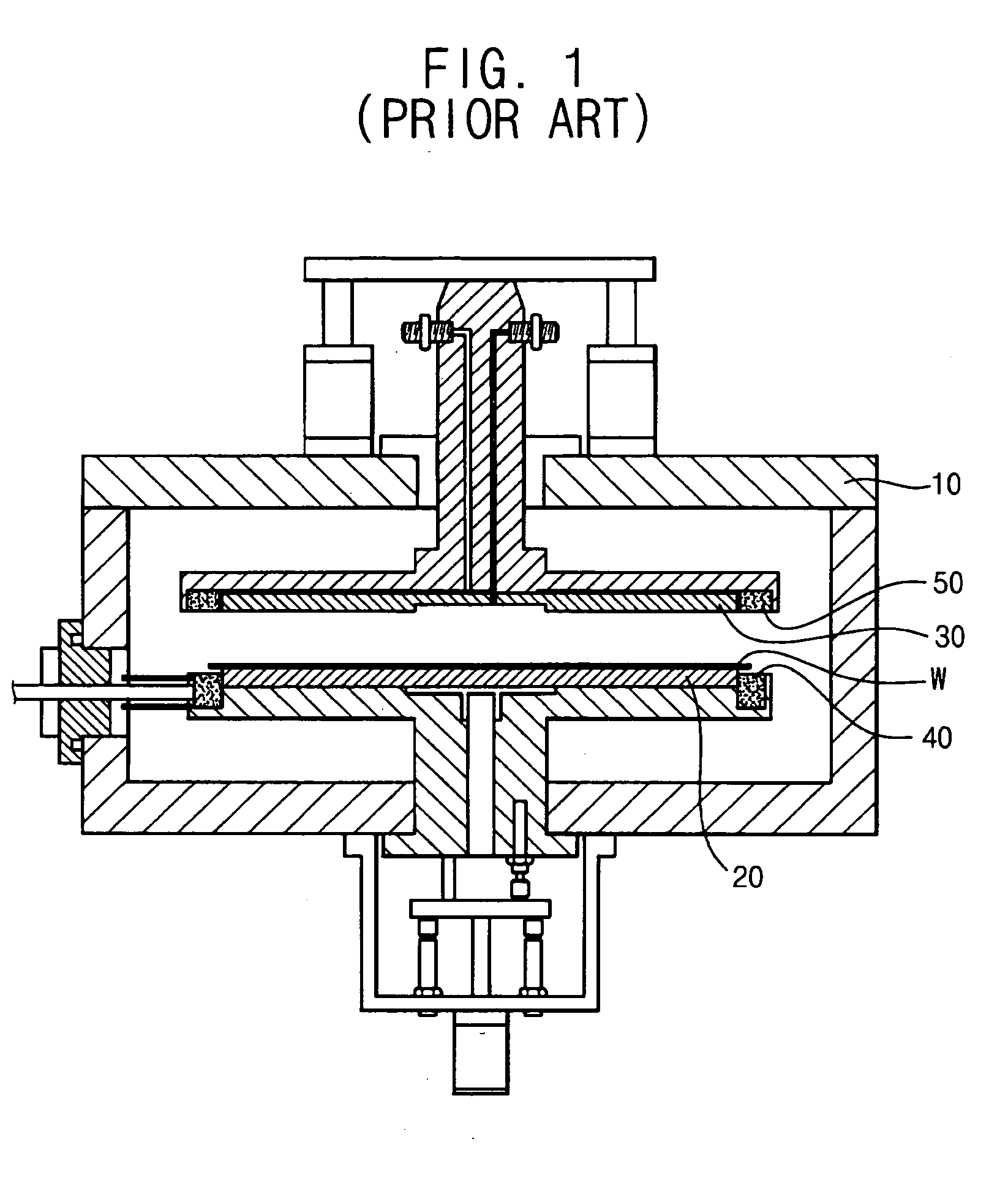
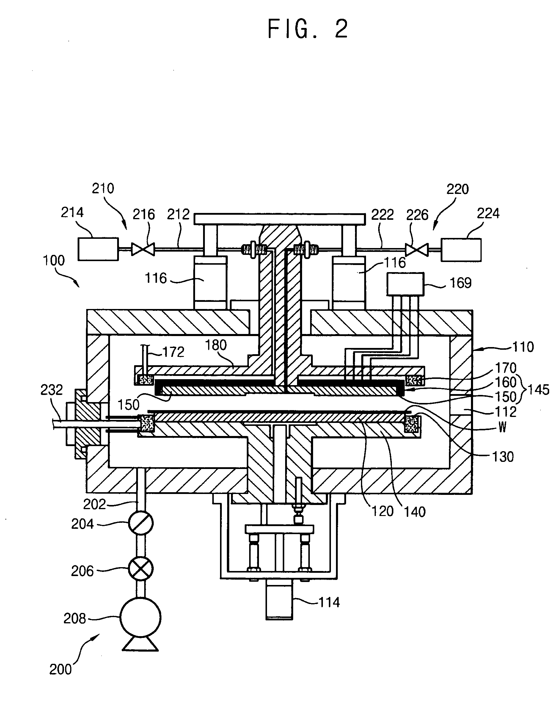
[0024] The present invention now is described more fully hereinafter with reference to the accompanying drawings, in which embodiments of the invention are shown. This invention may, however, be embodied in many different forms and should not be construed as limited to the embodiments set forth herein; rather, these embodiments are provided so that this disclosure will be thorough and complete, and will fully convey the scope of the invention to those skilled in the art.

[0025] Like numbers refer to like elements throughout. In the figures, the thickness of certain lines, layers, components, elements or features may be exaggerated for clarity.

[0026] The terminology used herein is for the purpose of describing particular embodiments only and is not intended to be limiting of the invention. As used herein, the singular forms “a”, “an” and “the” are intended to include the plural forms as well, unless the context clearly indicates otherwise. It will be further understood that the term...


PUM

PropertyMeasurementUnit
widthaaaaaaaaaa
areaaaaaaaaaaa
diametersaaaaaaaaaa

Abstract

An apparatus for adjusting an etching area of a semiconductor wafer includes an adjustable shielding plate. The adjustable shielding plate includes a plurality of shielding members. Each of the plurality of shielding members are movable between a first position configured to shield a portion of a semiconductor wafer from an etching gas and a second position configured to expose an unshielded etching portion of the semiconductor wafer to the etching gas.

Description

CROSS-REFERENCE TO RELATED APPLICATION [0001] This application claims priority to Korean Patent Application No. 2004-38891 filed on May 31, 2004, the content of which is herein incorporated by reference in its entirety. BACKGROUND OF THE INVENTION [0002] 1. Field of the Invention [0003] The present invention relates to methods and apparatus of fabricating a semiconductor device. More particularly, the present invention relates to methods and apparatus of etching an edge portion of a wafer for fabricating the semiconductor device. [0004] 2. Description of the Related Art [0005] As information and telecommunication technology improve, semiconductor technology has been developed to improve the integration degree, reliance and response speed of semiconductor devices. Single crystals of silicon may be formed on a silicon substrate, such as a silicon wafer, and various layers may be formed on the substrate. The various layers can be formed into patterns having desired electrical character...

Claims


Application Information

Patent Timeline
Patent Type & Authority Applications(United States)
IPC IPC(8): G01L21/30H01L21/3065H01J37/32H01L21/00H01L21/02
CPCH01J37/32623H01L21/67069H01L21/02087H01J2237/334H01L21/3065
Inventor PARK, JONG-CHULJEONG, SANG-SUP
Owner SAMSUNG ELECTRONICS CO LTD
Why Eureka
Try Eureka