Gallium nitride based light emitting device and the fabricating method for the same

a technology of light emitting diodes and gallium nitride, which is applied in the direction of basic electric elements, semiconductor devices, electrical equipment, etc., can solve the problems of poor light extraction efficiency, high cost, and difficult formation of roughening shapes, and achieve high light extraction efficiency

Inactive Publication Date: 2005-12-01
SEMILEDS OPTOELECTRONICS CO LTD
View PDF3 Cites 26 Cited by
  • Summary
  • Abstract
  • Description
  • Claims
  • Application Information

AI Technical Summary

Benefits of technology

[0010] The present invention is aimed to provide a GaN-based LED with high l

Problems solved by technology

However, a serious total reflection issue is closely related to the current spreading layer since the current spreading layer has flat surface and thus reflects light back to the LED structure and has a poor light extraction.

Method used


Image

  • Gallium nitride based light emitting device and the fabricating method for the same
  • Gallium nitride based light emitting device and the fabricating method for the same
  • Gallium nitride based light emitting device and the fabricating method for the same

Examples


Embodiment Construction

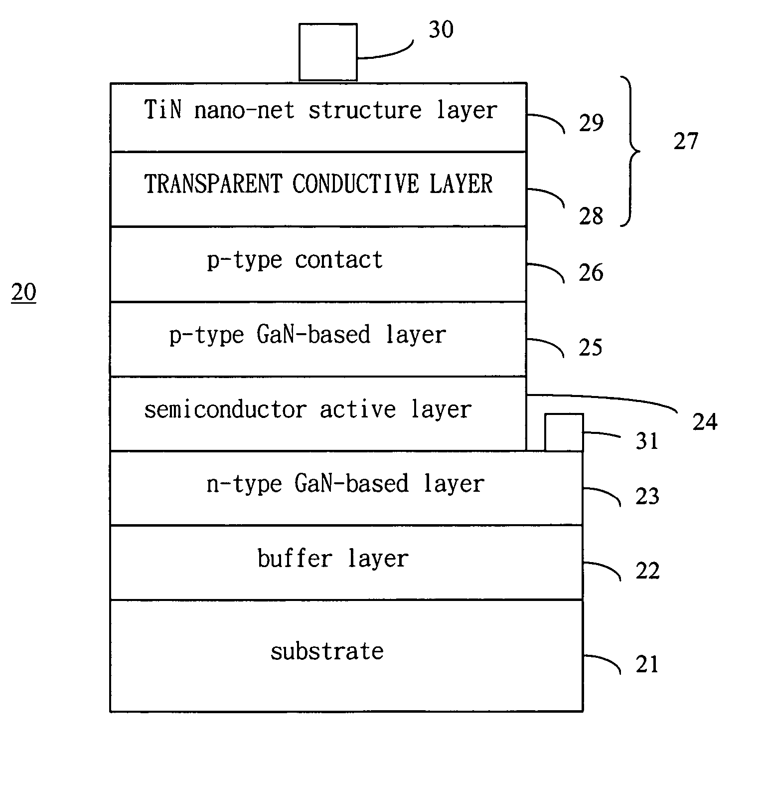
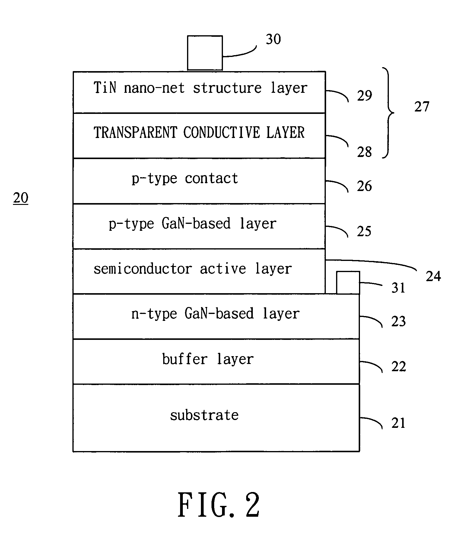
[0024] The present invention provides a light extraction layer with a micro-structure surface to reduce total reflection of light and enhance a light extraction efficiency of the light extraction layer, which is illustrated below.

[0025] The gallium nitride (GaN) light-emitting device (LED) primarily comprises two major embodiments. Referring to FIG. 2, which illustrates a first device structure 20 embodiment according to the present invention, a substrate 21 is first prepared, which may be sapphire, GaN or SiC or other suitable materials. An n-type GaN-based layer 23, a semiconductor active layer 24 and a p-type GaN-based layer 25 are sequentially formed over the substrate 21 to generate light when a voltage or a current is applied. The three layers 23, 24, 25 comprise a light-emitting body.

[0026] The semiconductor active layer may be an AlGaNInN layer or an InGaN / GaN layer. The substrate 21 and the n-type GaN-based layer 23 may be selectively disposed on a buffer layer 22 to let ...


PUM


Abstract

A GaN-based light-emitting device and the fabricating method for the same are described. The light-emitting device is a light-emitting body with a light extraction layer thereon. The light-emitting body has some GaN-based layers and is capable of emitting a light when energy is applied. The light extraction layer is a double layered structure having a current spreading layer and a micro-structure layer, or a single layered structure without the current spreading layer. The micro-structure layer is a TiN layer with a nano-net structure obtained by nitridation of a Ti layer or a Pt layer with metal clusters thereon obtained by annealing of a Pt layer.

Description

BACKGROUND OF THE INVENTION [0001] 1. Field of Invention [0002] The present invention is related to an improvement of luminous efficiency of a gallium nitride (GaN) based light-emitting diode (LED). in particular, the present invention is related to a GaN LED with a metal micro-structure as a light extraction layer and a manufacturing method for the same. [0003] 2. Related Art [0004] Semiconductor light-emitting diodes (LEDs) have been developed for several decades and the luminous efficiency thereof plays a key role in whether LEDs may be further applied in lighting facilities generally used in ordinary living. Therefore, LED research, for the past decades, has been focused on improvement of luminous efficiency. Generally, luminous efficiency varies with the following factors: semiconductor material adopted, device structure devised, transparency of material used, total reflection existed, etc. [0005] Of the semiconductor LEDs, a gallium nitride (GaN) based material may be the most...

Claims


Application Information

Patent Timeline
IPC IPC(8): H01L29/22H01L33/14H01L33/32H01L33/42
CPCH01L33/14H01L33/42H01L33/32
Inventor HON, SCHANG-JINGLAI, MU-JEN
Owner SEMILEDS OPTOELECTRONICS CO LTD
Why Eureka
Try Eureka