Semiconductor device and fabrication method therefor

a technology of semiconductor devices and fabrication methods, applied in semiconductor devices, electrical devices, transistors, etc., can solve the problems of difficult suppression excessive high voltage, and difficulty in suppressing the minute leakage current mentioned, etc., to suppress simple and easy process, effect of suppressing the occurrence of minute leakage curren

Inactive Publication Date: 2005-12-01
RENESAS TECH CORP
View PDF12 Cites 14 Cited by
  • Summary
  • Abstract
  • Description
  • Claims
  • Application Information

AI Technical Summary

Benefits of technology

[0011] The invention has been made in order to solve the task as described above and it is an object of the invention to provide a semiconductor device capable of suppressing occurrence of a minute leakage current. It is another object of the invention to provide a fabrication method for a semiconductor device capable of fabricating in a simple and easy process and suppressing occurrence of a minute leakage current.
[0020] According to a semiconductor device of the invention, a junction withstand voltage of the lower region of the drain region of the high withstand voltage transistor in the input protection circuit can be lower than an junction withstand voltage of the side end portion region of the drain region located on the gate electrode side of the high withstand voltage transistor. Hence, when a surge voltage is applied, electron-hole pairs can be formed at a voltage lower than the gate end portion below the drain of the high withstand voltage transistor in the input protection circuit, thereby enabling occurrence of electron-hole pairs to be suppressed at the gate end portion. Moreover, a parasitic bipolar transistor can be turned on by electron-hole pairs generated at the lower voltage. Hence, carrier injection into the gate insulating layer of the input protection circuit can be suppressed, thereby enabling occurrence of a minute current to be prevented.
[0021] In the fabrication method for a semiconductor device of the invention, since the first conductivity type impurity region is formed in the same fabrication step as the second well, no special step for forming the impurity region is unnecessary to be added and it is only required to change a pattern of a mask when the second well is formed. Therefore, a semiconductor device capable of suppressing occurrence a minute leakage current can be fabricated in a simple and easy process.
[0022] In the second fabrication method for a semiconductor device of the invention, since the high concentration region of the drain is fabricated simultaneously in the same fabrication step as the high concentration region of the source, no special step is necessary to be added in order to form the high concentration region of the drain and it is only required to change a pattern of a mask when the high concentration region of the source is formed. Therefore, a semiconductor device capable of suppressing occurrence of a minute current can be fabricated in a simple and easy process.

Problems solved by technology

A case arises where an excessively high voltage (a surge voltage) beyond a withstand voltage of an internal circuit is applied to an input / output terminal of a semiconductor device by static electricity.
Such an increase in minute leakage current has been problematic because of raised power consumption during standby.
Thus, it is difficult to suppress the minute leakage current mentioned above.
Even if the low withstand voltage transistor is applied to a construction without a p-type pocket region, a special fabrication step for forming the p-type diffused region is required, which makes a fabrication process complicated with difficulty of reduction in cost.

Method used


Image

  • Semiconductor device and fabrication method therefor
  • Semiconductor device and fabrication method therefor
  • Semiconductor device and fabrication method therefor

Examples


first embodiment

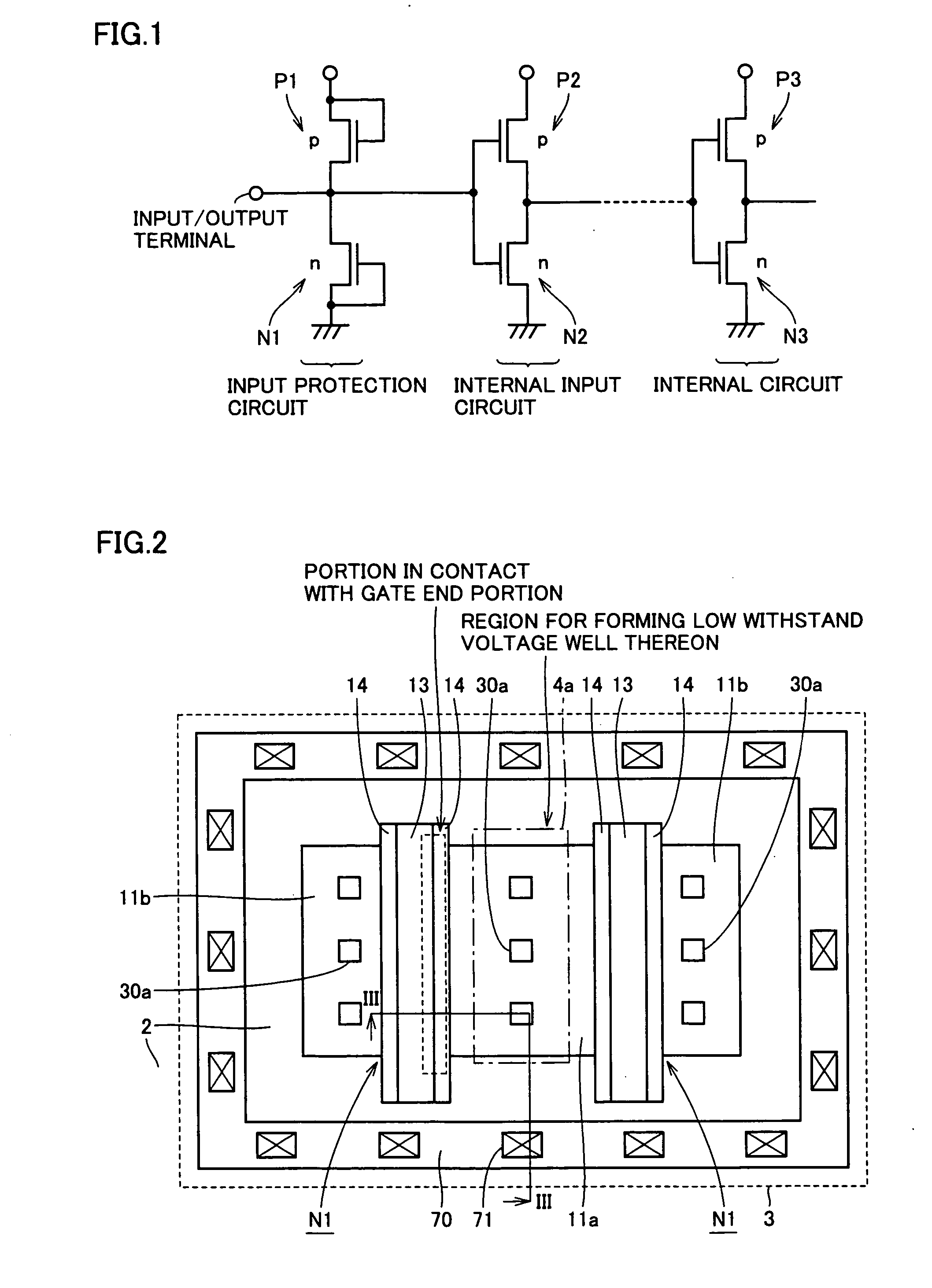
[0038]FIG. 1 is a circuit configuration in the vicinity of an input protection circuit of a semiconductor device in the first embodiment of the invention.

[0039] With reference to FIG. 1, an input protection circuit is disposed between an input / output terminal and an internal circuit. The input protection circuit is constituted of a CMOS (Complementary MOS) transistor circuit including, for example, an nMOS transistor N1 and a pMOS transistor P1. NMOS transistor N1 and pMOS transistor P1 are high withstand voltage transistors having a withstand voltage of 5 V or higher.

[0040] The source and gate of nMOS transistor N1 are electrically connected to a ground (GND) potential, the source and gate of pMOS transistor P1 are electrically connected to a power supply potential and the drains of nMOS transistor N1 and pMOS transistor P1 are electrically connected to each other.

[0041] The input / output terminal and the internal circuit both are electrically connected to the drains of nMOS tran...

second embodiment

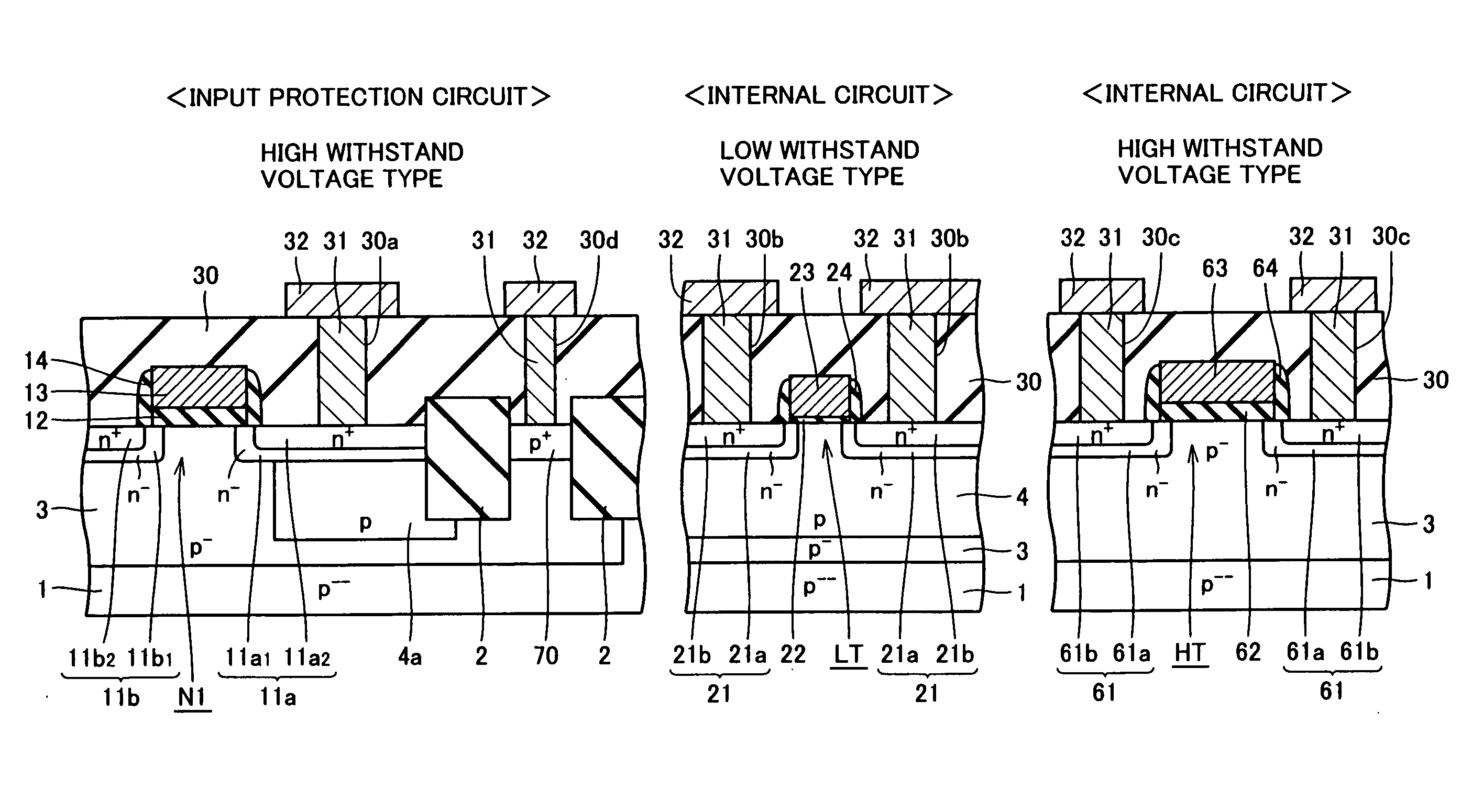
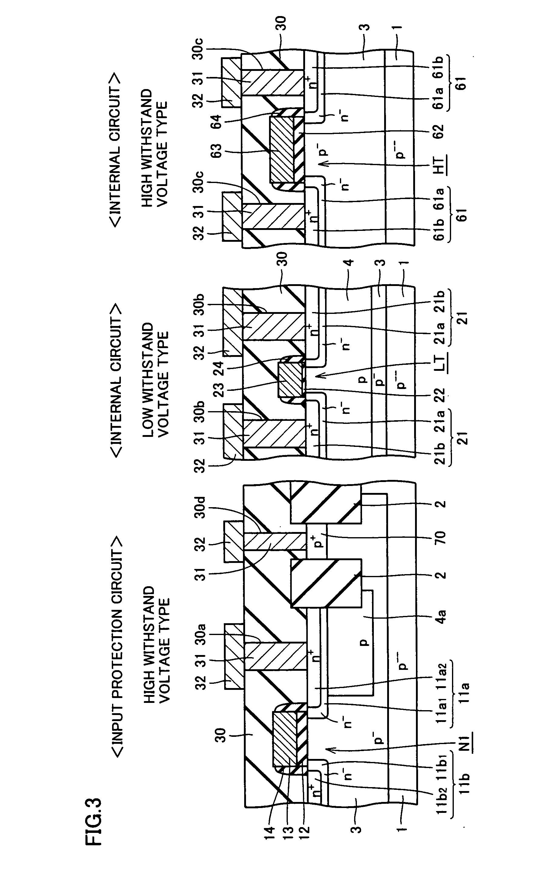
[0092]FIG. 14 is schematic sectional views of a high withstand voltage nMOS transistor included in an input protection circuit of a semiconductor device, and a low withstand voltage nMOS transistor and a high withstand voltage nMOS transistor included in a internal circuit of a semiconductor device in the second embodiment of the invention, wherein a sectional view of the high withstand nMOS transistor included in the input protection circuit corresponds to the sectional view taken along line III-III of FIG. 2.

[0093] With reference to FIG. 14, p− high withstand well 3 is formed on p−− semiconductor substrate in a region for forming a low withstand voltage transistor LT thereon included in the internal circuit and p-type low withstand well 4 is formed on p− high withstand well 3. A pair of n-type impurity regions working as source region 21 and drain region 21, respectively, are formed on a surface of p-type low withstand voltage well 4. A pair of n-type impurity regions 21 and 21 e...


PUM


Abstract

A high withstand voltage well is formed on a surface of a semiconductor substrate. A drain region and a source region of a high withstand voltage transistor included in an input protection circuit are formed on the high withstand voltage well. A p-type impurity region is formed adjacent to the lower portion of the drain region of the high withstand voltage transistor. The p-type impurity region is fabricated in the same fabrication step as a low withstand voltage well formed in a region on which a low withstand voltage transistor is formed.

Description

BACKGROUND OF THE INVENTION [0001] 1. Field of the Invention [0002] The invention relates to a semiconductor device and a fabrication method therefor, and in particular, to a semiconductor device having an input protection circuit disposed between an input / output terminal and an internal circuit and a fabrication method therefor. [0003] 2. Description of the Background Art [0004] A case arises where an excessively high voltage (a surge voltage) beyond a withstand voltage of an internal circuit is applied to an input / output terminal of a semiconductor device by static electricity. If an excessively high voltage is applied directly to the internal circuit, the internal circuit is broken down. [0005] In order to prevent breakdown of the internal circuit, the input protection circuit has been provided between the input / output terminal and the internal circuit. With the input protection circuit adopted, when an excessively high voltage is applied to the input / output terminal, a current f...

Claims


Application Information

Patent Timeline
Patent Type & Authority Applications(United States)
IPC IPC(8): H01L21/336H01L21/8238H01L27/02H01L27/092H01L29/00
CPCH01L21/823814H01L21/823857H01L27/0922H01L27/0266H01L21/823892H01L27/04
Inventor SAKAKIBARA, KIYOHIKO
Owner RENESAS TECH CORP
Why Eureka
Try Eureka