Omnidirectional photonic crystal

Inactive Publication Date: 2005-12-01
LIN CHUNG HSIANG
View PDF2 Cites 31 Cited by
  • Summary
  • Abstract
  • Description
  • Claims
  • Application Information

AI Technical Summary

Benefits of technology

[0009] The object of the present invention is to provide an omnidirectional photonic crystal that is useful for optical filters and that is capable of overcoming the aforesaid drawbacks associated with the prior art.
[0010] According to this invention, an omnidirectional photonic crystal comprises: a substrate; and a periodic dielectric structure that is formed on the substrate and that includes a stack of dielectric units. Each of the dielectric units includes upper and lower dielectric slabs and at least one intermediate dielectric slab sandwiched between the upper and lower dielectric slabs. The periodic dielectric structure introduces an omnidirectional photonic band gap in a given frequency range such that radiation at the frequency range for all incident angles and polarizations can be totally reflected by the omnidirectional photonic crystal. The upper and lower dielectric slabs of each of the dielectric units are made from a first dielectric material. The intermediate dielectric slab of each of the dielectric units is made from a second dielectric material that has a refractive index smaller than that of the first dielectric material. The periodic dielectric structure defines a lattice constant a that is equal to the total thickness of each of the dielectric units. The intermediate dielectric slab of each of the dielectric units has a thickness d, the upper dielectric slab of each of the dielectric units has a thickness equal to x(a−d), and the lower dielectric slab of each of the dielectric units has a thickness equal to (1−x) (a−d), where x is a positive number ranging from 0.2 to 0.8.

Problems solved by technology

However, the conventional optical filters are disadvantageous in that when the incident angle of the incoming light is broad, undesired frequencies outside the frequency range of interest also pass through the conventional optical filters.

Method used


Image

  • Omnidirectional photonic crystal
  • Omnidirectional photonic crystal
  • Omnidirectional photonic crystal

Examples


example 1

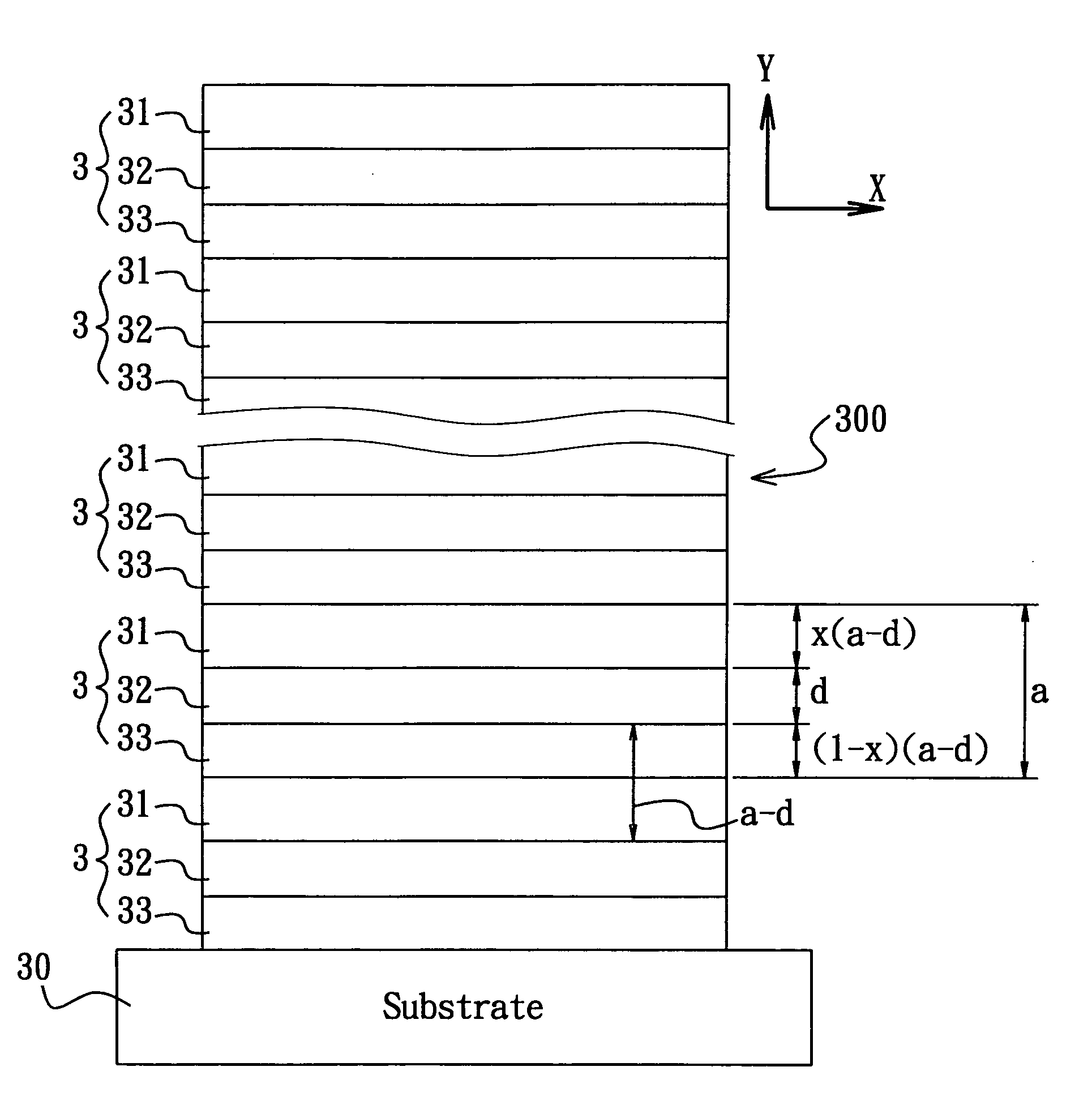
[0024] The periodic dielectric structure 300 of the omnidirectional photonic crystal of this Example includes fourteen stacked dielectric units 3, each including the upper and lower dielectric slabs 31, 33 and one intermediate dielectric slab 32, with n1=2.7 (TiO2), n2=1.5 (SiO2), n3=1.0 (substrate 30), d=0.5a, and x=0.5, and introduces an omnidirectional photonic band gap in a frequency range between 0.248c / a and 0.276c / a, where c is the speed of light, or in a wavelength range between 3.6a and 4.0a. Note that the width and the location (i.e., the frequency range) of the omnidirectional photonic band gap will not vary with x. Transmittance of the omnidirectional photonic crystal of this Example in a given range of wavelength λ is calculated for different values of x. The results are shown in FIG. 4.

[0025] When the wavelength λ is less than about 4.7a (see FIG. 4), the transmittance of the omnidirectional photonic crystal almost remains the same and does not change with the shiftin...

example 2

[0026] The periodic dielectric structure 300 of the omnidirectional photonic crystal of this Example differs from the previous Example in that n3=1.5. Transmittance of the omnidirectional photonic crystal of this Example in a given range of wavelength λ is calculated for different values of x. The results are shown in FIG. 5.

[0027] The behavior of the variation of transmittance with x for the omnidirectional photonic crystal of this example is similar to that of the previous Example. The highest transmittance for all the wavelength greater than about 5.0a occurs at x=0.5.

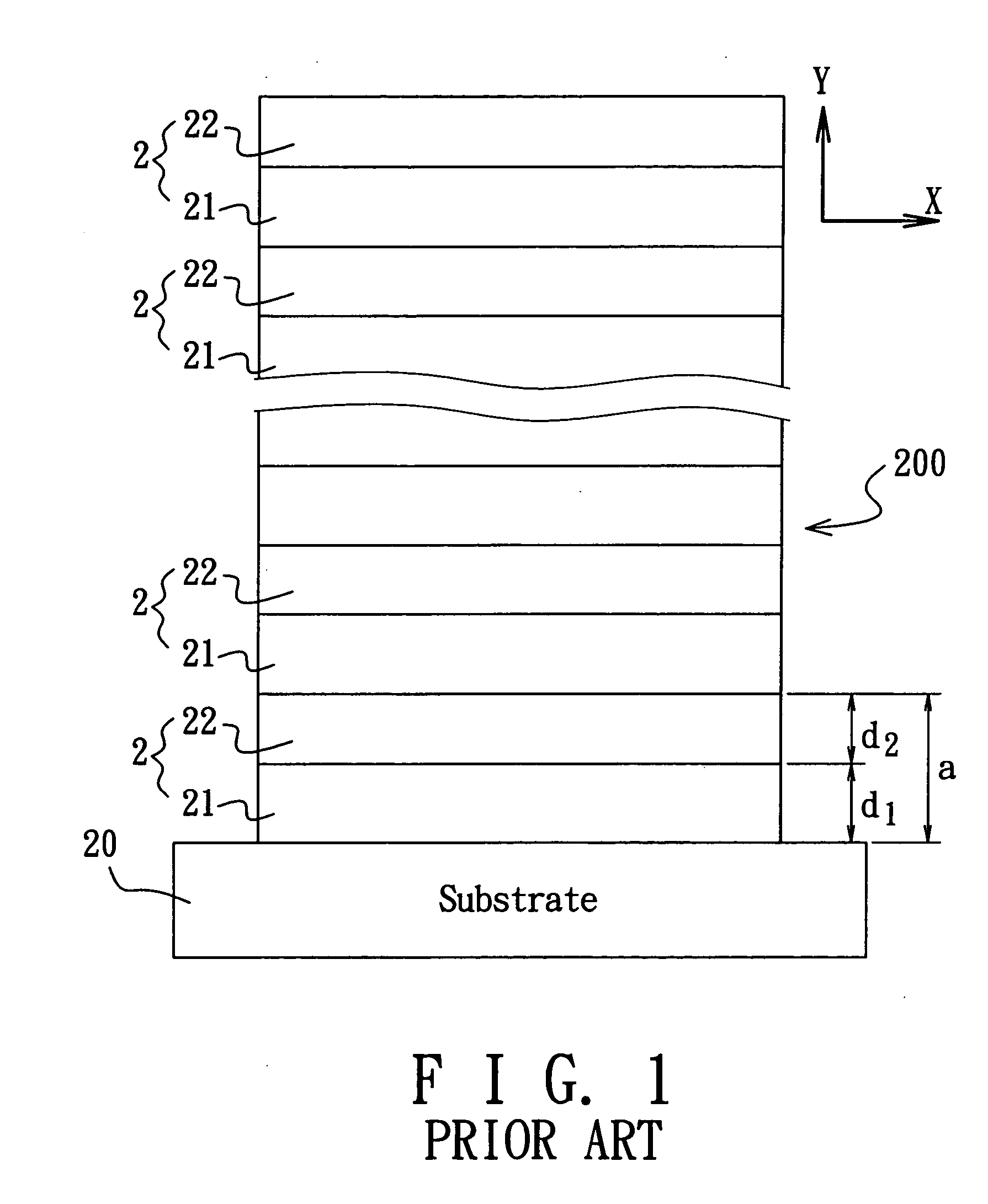
[0028]FIG. 6 is a plot showing comparison of the average reflectance (an inversion of the transmittance) among the omnidirectional photonic crystal (solid line) of the preferred embodiment with x=0.5, a=102 nm, and d=44 nm (the intermediate dielectric slab 32 is SiO2, and the upper and lower dielectric slabs 31, 32 are TiO2), the conventional omnidirectional photonic crystal of FIG. 1 (dotted line, x=0), and the o...


PUM


Abstract

An omnidirectional photonic crystal includes a substrate and a periodic dielectric structure that is formed on the substrate and that includes a stack of dielectric units. Each of the dielectric units includes upper and lower dielectric slabs and at least one intermediate dielectric slab sandwiched between the upper and lower dielectric slabs. The periodic dielectric structure introduces an omnidirectional photonic band gap in a given frequency range. The periodic dielectric structure defines a lattice constant a that is equal to the total thickness of each of the dielectric units. The intermediate dielectric slab has a thickness d, the upper dielectric slab has a thickness equal to x(a−d), and the lower dielectric slab has a thickness equal to (1−x) (a−d), where x is a positive number ranging from 0.2 to 0.8.

Description

BACKGROUND OF THE INVENTION [0001] 1. Field of the Invention [0002] This invention relates to an omnidirectional photonic crystal, more particularly to an omnidirectional photonic crystal useful for optical filters. [0003] 2. Description of the Related Art [0004] Conventional optical filters, such as long-wavelength pass filters and short-wavelength pass filters, include a multi-layered dielectric structure that is capable of rejecting radiation falling outside of the frequency range of interest from passing therethrough. However, the conventional optical filters are disadvantageous in that when the incident angle of the incoming light is broad, undesired frequencies outside the frequency range of interest also pass through the conventional optical filters. [0005] U.S. Pat. No. 6,130,780 discloses a highly omnidirectional reflector made from an omnidirectional photonic crystal that includes a periodic photonic structure with a surface and a refractive index variation along a directi...

Claims


Application Information

Patent Timeline
Patent Type & Authority Applications(United States)
IPC IPC(8): G02B5/08G02B5/20G02B6/122
CPCG02B6/1225B82Y20/00
Inventor LIN, CHUNG-HSIANG
Owner LIN CHUNG HSIANG
Why Eureka
Try Eureka