Semiconductor memory device

a memory device and semiconductor technology, applied in the direction of digital storage, instruments, transistors, etc., can solve the problems of the wiring capacity of each main bit line counterbalancing with each other, and achieve the effects of preventing the lowering of the readout operation margin, reducing the detour outflow current through adjacent non-selected memory cells, and avoiding the delay in readout access tim

Inactive Publication Date: 2005-12-01
SHARP KK
View PDF1 Cites 95 Cited by
  • Summary
  • Abstract
  • Description
  • Claims
  • Application Information

AI Technical Summary

Benefits of technology

[0029] According to the semiconductor memory device of the present invention, since the number of the selection transistors connected to the first main bit line is the same as that connected to the second main bit line which are common in each sub-array positioned in the same column, the total junction capacities of the selection transistors contained in the wiring capacities of the main bit lines are the same. As a result, the wiring capacity of each main bit line counterbalances with each other. That is, even when either the first main bit line or the second main bit line becomes the main bit line to read out the data, depending on the column position of the selected memory cell or the selected bit of the multi-level memory cell, the charging and discharging times of the main bit lines become the same, so that a delay in readout access time caused by the fluctuation in charging and discharging time between the main bit lines can be avoided.
[0030] Here, even if the number of the sub-arrays positioned in the same column is the odd number (2k+1, for example), when its half is set at k (or k+1) and the other half is set at k+1 (or k), the difference of the wiring capacity between the main bit lines can be reduced to be a junction capacity of one selection transistor, so that the same effect as in the case the number of the sub-arrays positioned in the same column is the even number can be provided.
[0031] The semiconductor

Problems solved by technology

As a result, the wiring capacity of each ma

Method used


Image

  • Semiconductor memory device
  • Semiconductor memory device
  • Semiconductor memory device

Examples


embodiment 1

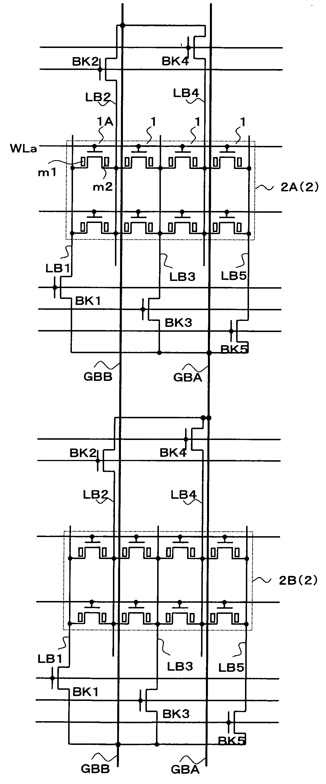
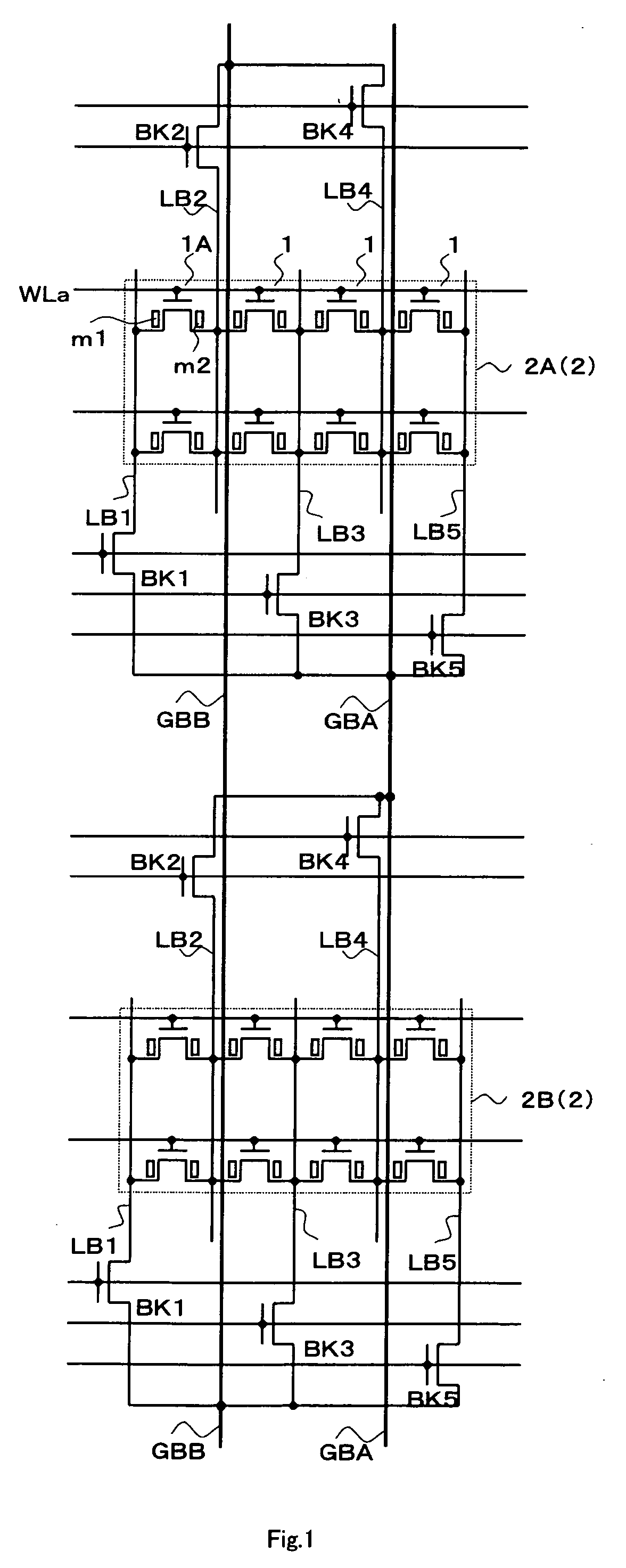
[0043]FIG. 1 is a circuit diagram simply showing a memory cell array structure of the device of the present invention. According to the memory cell array in the device of the present invention, a sub-array 2 is provided such that memory cells 1 are arranged with even numbers in rows and with plural numbers in columns in the shape of an array, and the sub-arrays 2 are arranged with plural numbers in rows and columns. FIG. 1 shows two sub-arrays 2A and 2B which are adjacent to each other in the column direction. Although the number of columns (the number of arrangements in the row direction) of the memory cells of each sub-array 2 shown in FIG. 1 is four, it may be another even number such as eight or sixteen other than four.

[0044] The memory cell 1 is a non-volatile memory cell comprising a gate electrode (a first electrode), a source electrode (one of second electrodes) and a drain electrode (the other of the second electrodes), and having a MOSFET structure in which memory content...

embodiment 2

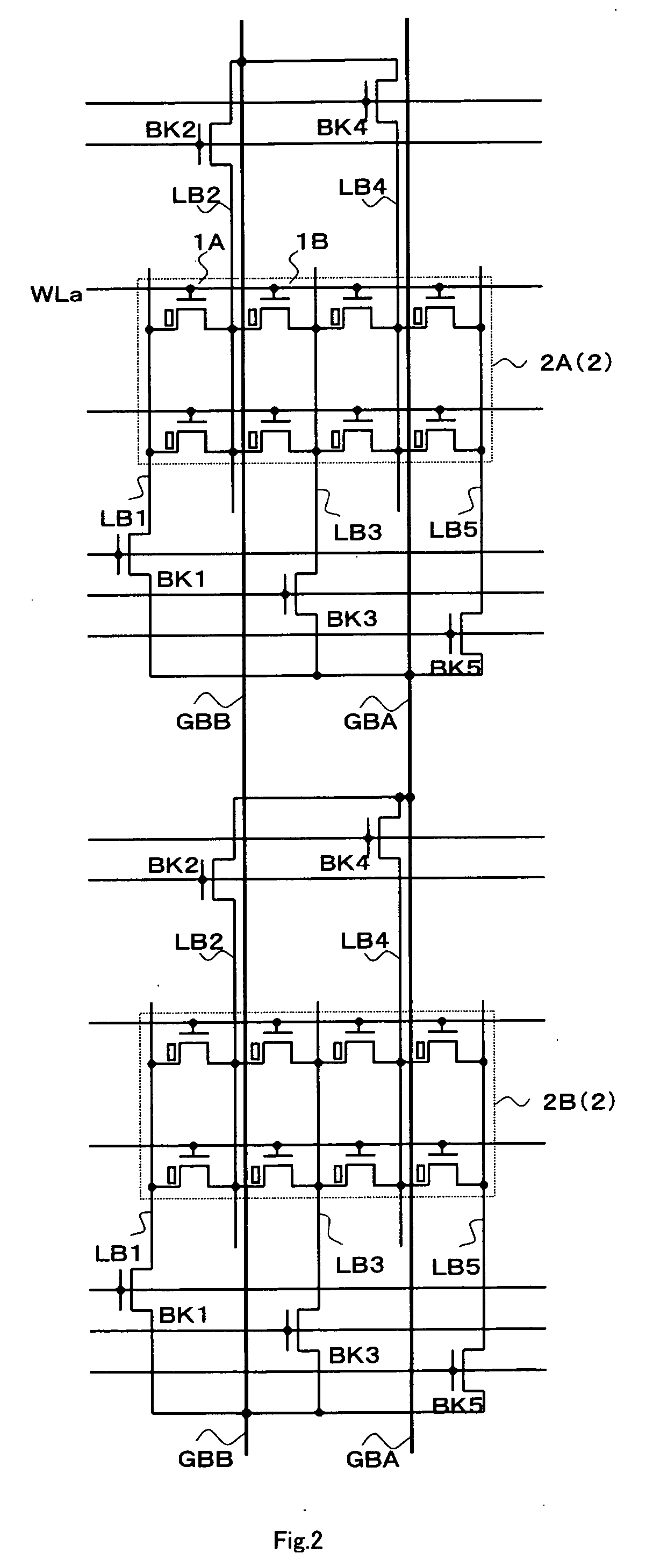
[0049]FIG. 2 is a circuit diagram simply showing a memory cell array structure of a device of the present invention according to an embodiment 2. According to the memory cell array in the device of the present invention, a sub-array 2 is provided such that memory cells 1 are arranged with even numbers in rows and with plural numbers in columns in the shape of an array, and the sub-arrays 2 are arranged with plural numbers in rows and columns. FIG. 2 shows two sub-arrays 2A and 2B which are adjacent to each other in the column direction. Although the number of columns (the number of arrangements in the row direction) of the memory cells of each sub-array 2 shown in FIG. 2 is four, it may be another even number such as eight or sixteen other than four.

[0050] The memory cell 1 is a non-volatile memory cell comprising a gate electrode (a first electrode), a source electrode (one of second electrodes) and a drain electrode (the other of the second electrodes), and having a MOSFET struct...


PUM


Abstract

In a memory cell array in a hierarchical bit line mode in which sub-arrays in a virtual ground line mode are arranged in a column direction, data is read out at high speed, preventing fluctuation in wiring capacity of a main bit line. In each sub-array, one of a source electrode or a drain electrode in each of the memory cells in the same column is connected to a common first bit line, and the other thereof is connected to a second bit line. The first bit lines of one half of the sub-arrays positioned in the same column are connected to the first main bit line through selection transistors and the second bit lines thereof are connected to the second main bit line through selection transistors, and the first bit lines of the other half of the sub-arrays positioned in the same column are connected to the second main bit line through selection transistors and the second bit lines thereof are connected to the first main bit line through selection transistors.

Description

CROSS REFERENCE TO RELATED APPLICATTION [0001] This Nonprovisional application claims priority under 35 U.S.C. §119(a) on Patent Application No. 2004-161668 filed in Japan on May 31, 2004, the entire contents of which are hereby incorporated by reference. BACKGROUND OF THE INVENTION [0002] 1. Field of the Invention [0003] The present invention relates to a semiconductor memory device and more particularly, it relates to a semiconductor memory device comprising a memory cell array in a virtual ground line mode which employs a memory cell array structure in a hierarchical bit line mode comprising a main bit line and a sub-bit line. [0004] 2. Description of the Related Art [0005] Conventionally, there is a mode in which a memory cell is read out using a bit line and a virtual ground line in a non-volatile semiconductor memory device such as a mask ROM (mask programmable read only memory) and a flush memory (refer to Japanese Unexamined Patent Publication No. 10-11991, and Japanese Unex...

Claims


Application Information

Patent Timeline
IPC IPC(8): G11C16/04G11C7/18G11C8/00G11C16/02G11C16/06G11C16/24H01L21/8247H01L27/115H01L29/788H01L29/792
CPCG11C7/18G11C2207/002G11C16/24
Inventor TANAKA, TOMOYA
Owner SHARP KK
Why Eureka
Try Eureka