Compact semiconductor-based chirped-pulse amplifier system and method

a semiconductor and amplifier technology, applied in the field of optical systems, can solve problems such as significant nonlinear pulse distortion and/or damage or destroy the semiconductor gain medium

Inactive Publication Date: 2005-12-01
BRAUN ALAN MICHAEL +1
View PDF0 Cites 91 Cited by
  • Summary
  • Abstract
  • Description
  • Claims
  • Application Information

AI Technical Summary

Problems solved by technology

However, when generating and amplifying short optical pulses using semiconductor-based sources, optical peak intensities may conventionally be sufficiently high to cause significant nonlinear pulse distortion and / or damage or destroy the semiconductor gain medium.

Method used


Image

  • Compact semiconductor-based chirped-pulse amplifier system and method
  • Compact semiconductor-based chirped-pulse amplifier system and method
  • Compact semiconductor-based chirped-pulse amplifier system and method

Examples


Embodiment Construction

[0015] It is to be understood that the figures and descriptions of the present invention have been simplified to illustrate elements that are relevant for a clear understanding of the present invention, while eliminating, for purposes of clarity, many other elements found in typical optical systems and methods of making and using the same. Those of ordinary skill in the art will recognize that other elements are desirable and / or required in order to implement the present invention. However, because such elements are well known in the art, and because they do not facilitate a better understanding of the present invention, a discussion of such elements is not provided herein.

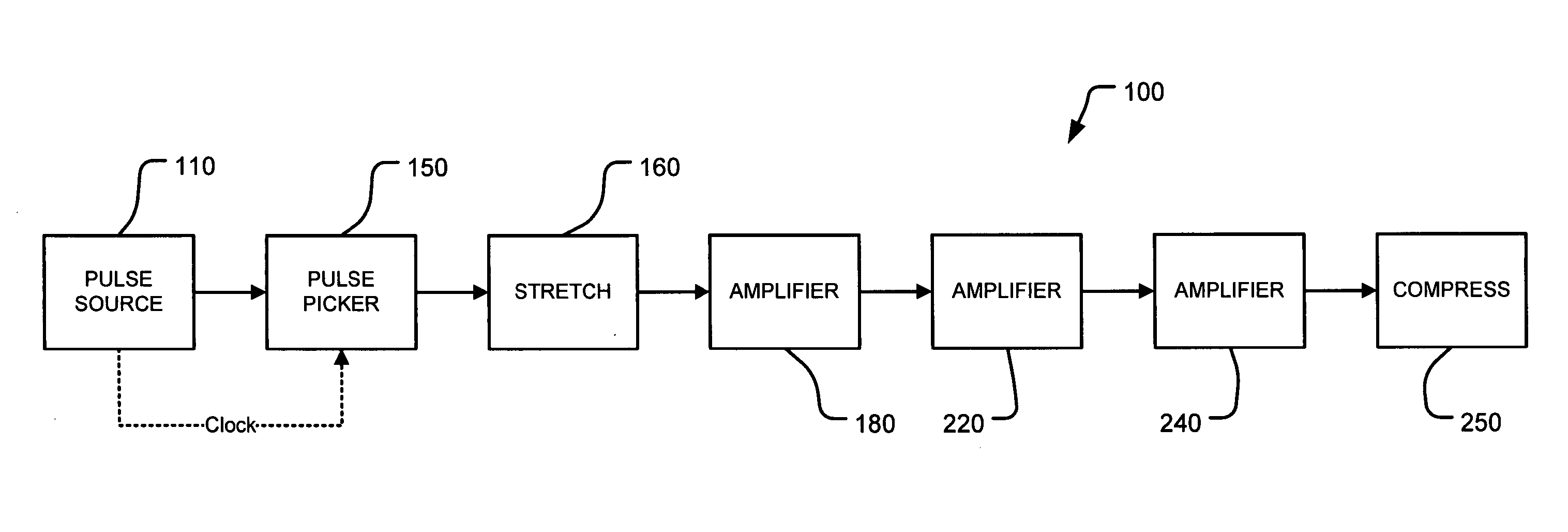
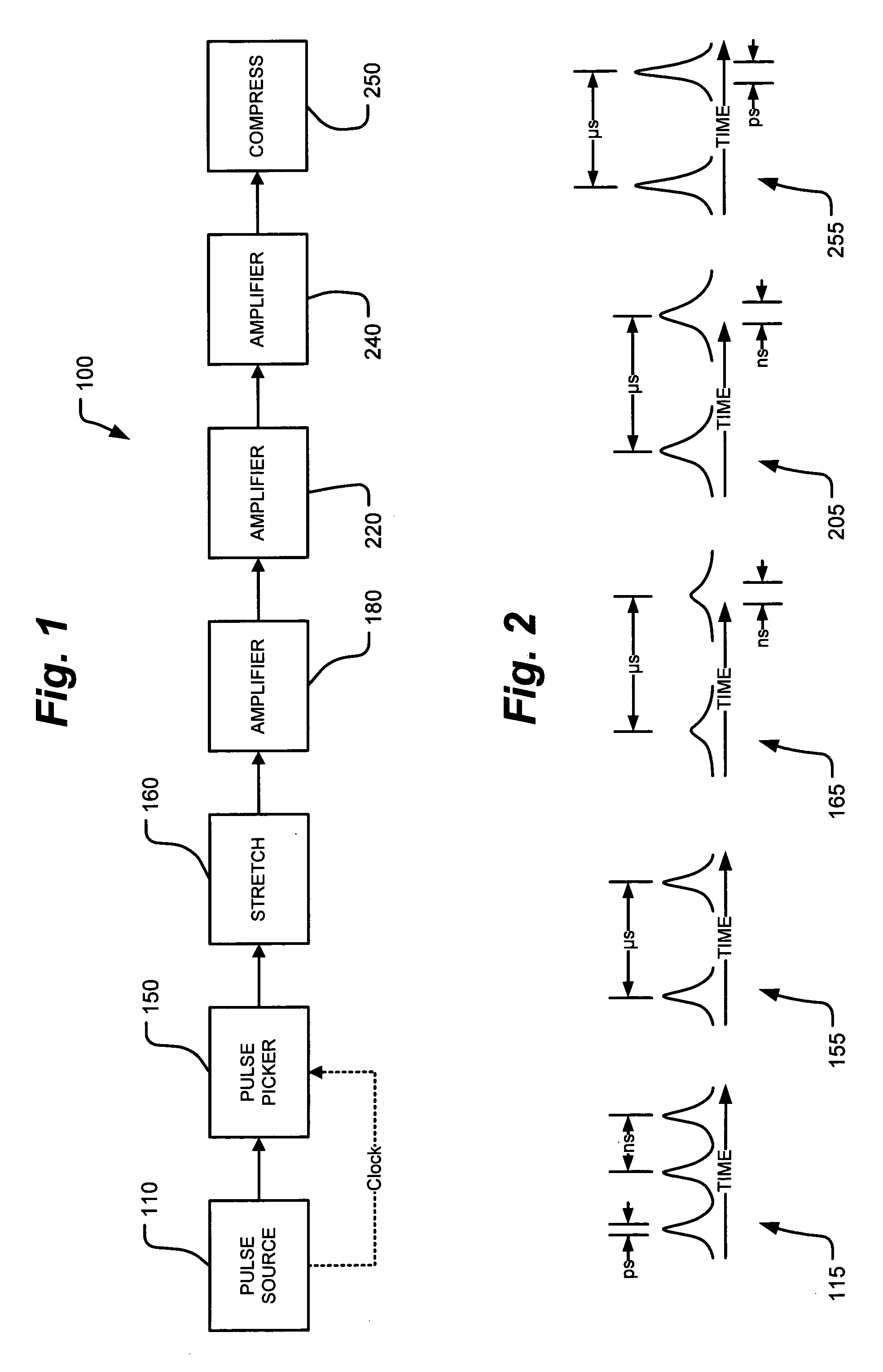
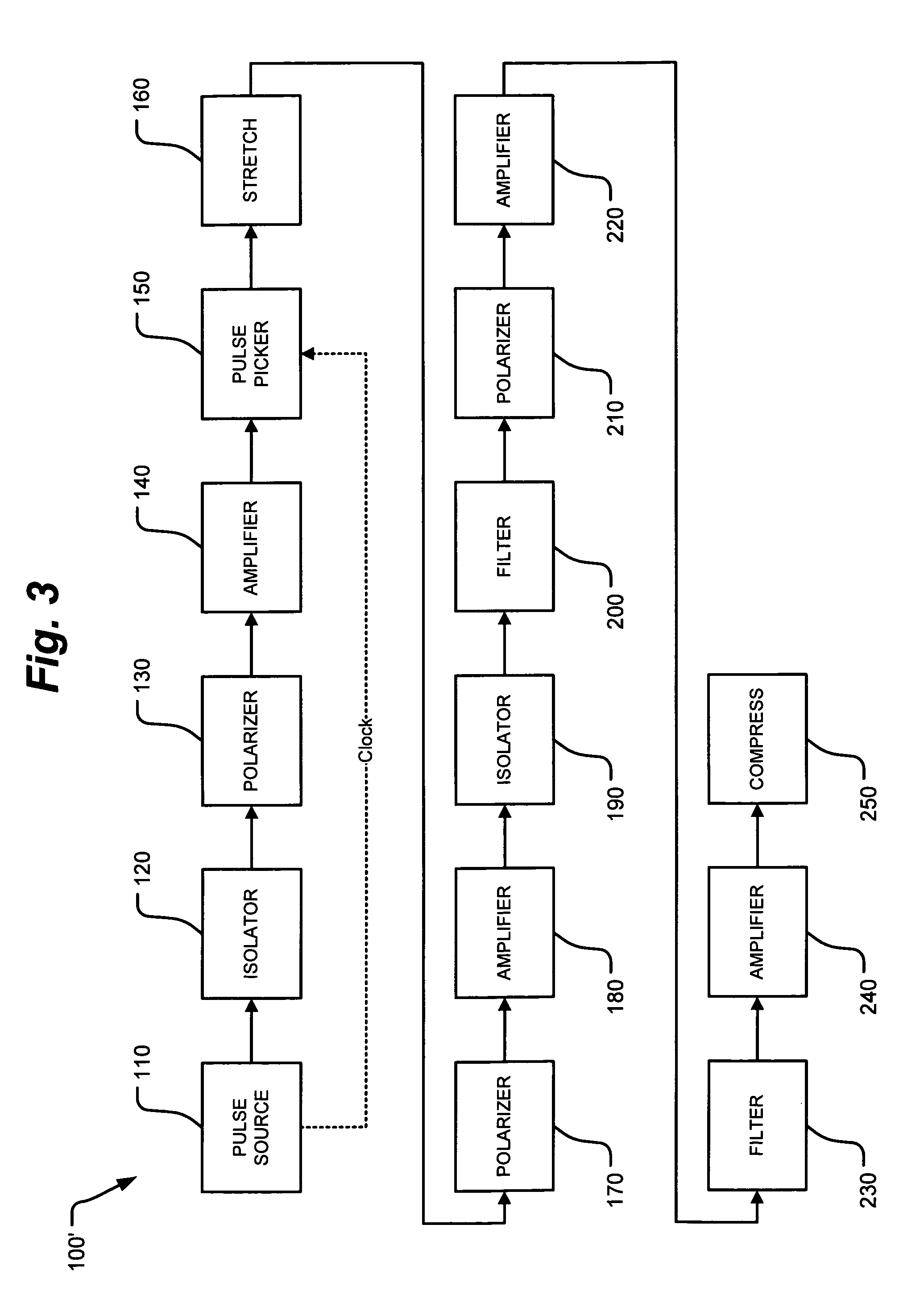
[0016] According to an aspect of the present invention, chirped pulse amplification (CPA) may be used in combination with a semiconductor-based (e.g., diode) laser source to provide a high peak power, short duration optical pulse generating laser system. CPA may be used to provide high peak power laser pulses by ...


PUM


Abstract

A compact signal source including: a semiconductor-based, pulsed optical energy source for providing a series of pulses at a given frequency; a selector being optical fiber coupled to the pulsed optical energy source and for down-selecting the pulses to a lower frequency; a stretcher being optical fiber coupled to the selector and for temporally stretching the selected pulses; at least one semiconductor-based optical amplifier being optical fiber coupled to the stretcher and for amplifying the selected pulses; a compressor being optical fiber coupled to the at least one semiconductor-based amplifier and for temporally compressing the amplified, stretched, selected pulses; and, a portable housing containing the pulsed optical energy source, stretcher, at least one semiconductor-based optical amplifier and compressor.

Description

RELATED APPLICATIONS [0001] This Application claims priority of U.S. patent application Ser. No. 60 / 571,355, filed May 15, 2004, entitled COMPACT SEMICONDUCTOR-BASED CHIRPED-PULSE AMPLIFICATION SYSTEM, and is a continuation-in-part application of U.S. patent application Ser. No. 10 / 859,553, filed Jun. 1, 2004 entitled COMPACT, HIGH-POWER, LOW-JITTER, SEMICONDUCTOR MODELOCKED LASER MODULE, the entire disclosures of each of which are hereby incorporated by reference as if being set forth in their respective entireties herein.GOVERNMENT RIGHTS [0002] This invention was made with Government support under Contract No. MDA-972-03-C-0043 awarded by DARPA. The Government has certain rights in this invention.FIELD OF INVENTION [0003] The present invention relates generally to optical systems, and more particularly to photonic systems. BACKGROUND OF THE INVENTION [0004] Semiconductor-based optical sources are desired in many applications, due in part to their compact and transportable nature,...

Claims


Application Information

Patent Timeline
Patent Type & Authority Applications(United States)
IPC IPC(8): H01S3/00H01S3/067H01S3/10H01S3/16H01S3/23H01S5/00H01S5/022H01S5/40
CPCH01S3/0057H01S3/0078H01S3/025H01S3/06754H01S3/06758H01S5/4006H01S3/2316H01S5/0057H01S5/0064H01S5/0085H01S3/1608
Inventor BRAUN, ALAN MICHAELDELFYETT, PETER J.
Owner BRAUN ALAN MICHAEL
Why Eureka
Try Eureka