Methods of forming non-volatile memory cells including fin structures and related devices

a non-volatile memory and fin structure technology, applied in the field of non-volatile memory devices and methods, can solve the problems of increasing the operating voltage of small flash memory cells, increasing the power dissipation, and affecting the operation of flash memory cells, so as to reduce the operating voltage, increase the turn-on current and increase the integration densities of non-volatile memory cells

Inactive Publication Date: 2005-12-01
SAMSUNG ELECTRONICS CO LTD
View PDF13 Cites 78 Cited by
  • Summary
  • Abstract
  • Description
  • Claims
  • Application Information

AI Technical Summary

Benefits of technology

[0015] According to some embodiments of the present invention, a turn-on current of a non-volatile memory cell may be increased while reducing an operating voltage thereof, and / or integration densities of non-volatile memory cells may be increased.

Problems solved by technology

For these reasons, smaller flash memory cells may require higher operating voltages, and power dissipation may thus be increased.
Moreover, an interface between the tunnel oxide layer 2 and the active region may be damaged by higher operating voltages, and reliability of the flash memory cell may be reduced.

Method used


Image

  • Methods of forming non-volatile memory cells including fin structures and related devices
  • Methods of forming non-volatile memory cells including fin structures and related devices
  • Methods of forming non-volatile memory cells including fin structures and related devices

Examples


Embodiment Construction

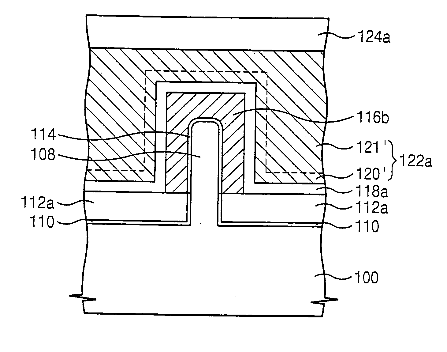
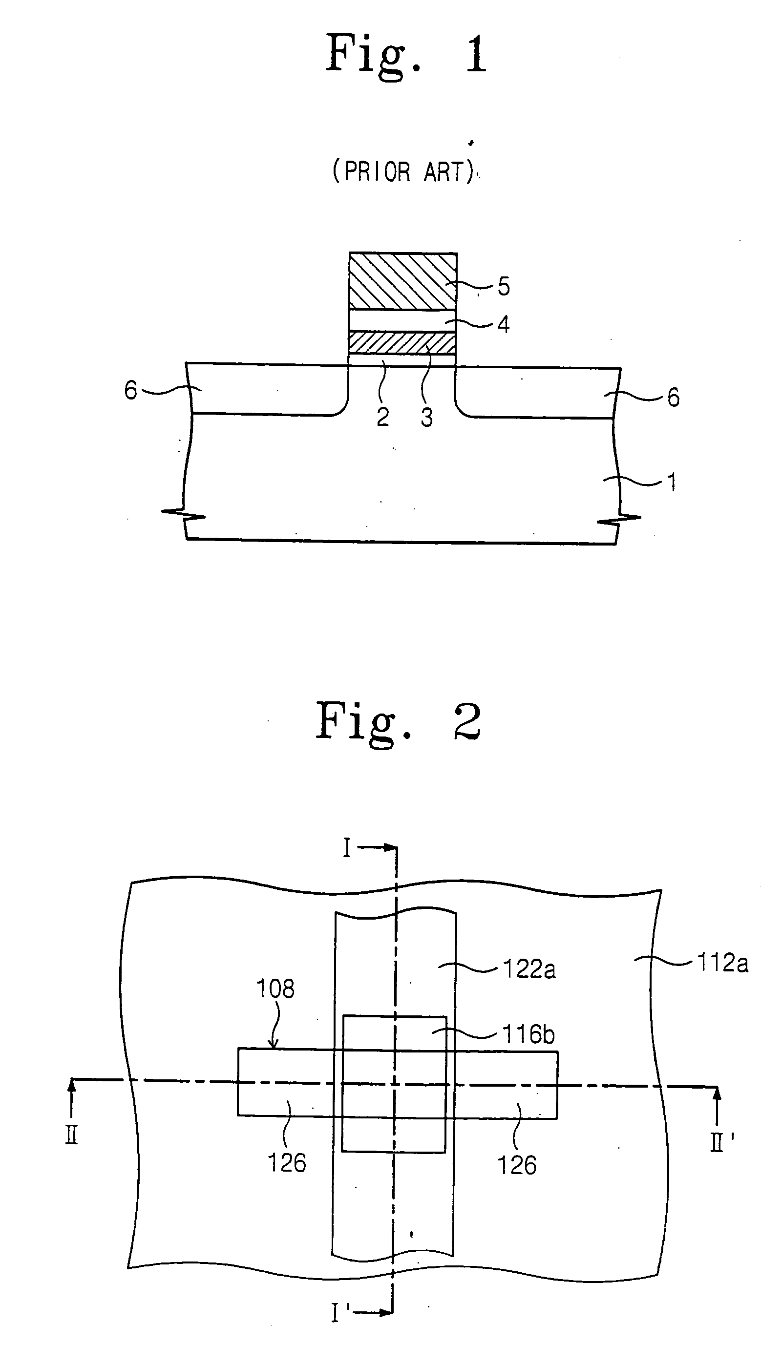
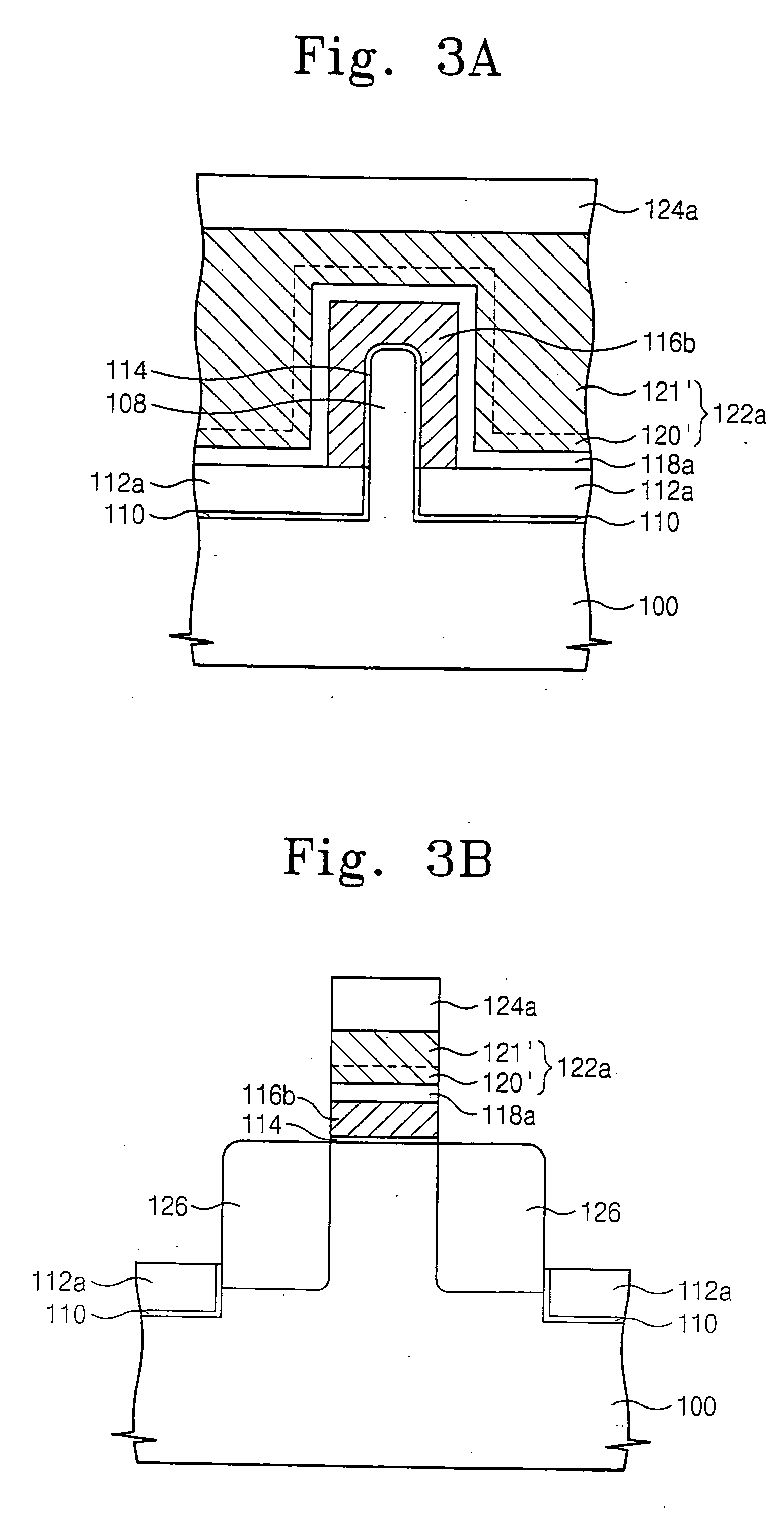
[0036] The present invention now will be described more fully hereinafter with reference to the accompanying drawings, in which embodiments of the invention are shown. This invention may, however, be embodied in many different forms and should not be construed as limited to the embodiments set forth herein. Rather, these embodiments are provided so that this disclosure will be thorough and complete, and will fully convey the scope of the invention to those skilled in the art.

[0037] In the drawings, the thickness of layers and regions are exaggerated for clarity. It will also be understood that when an element such as a layer, region or substrate is referred to as being on another element, it can be directly on the other element or intervening elements may also be present. In contrast, if an element such as a layer, region or substrate is referred to as being directly on another element, then no other intervening elements are present. As used herein, the term and / or includes any and...


PUM


Abstract

A method of forming a non-volatile memory device may include forming a fin protruding from a substrate, forming a tunnel insulating layer on portions of the fin, and forming a floating gate on the tunnel insulting layer so that the tunnel insulating layer is between the floating gate and the fin. A dielectric layer may be formed on the floating gate so that the floating gate is between the dielectric layer and the fin, and a control gate electrode may be formed on the dielectric layer so that the dielectric layer is between the control gate and the fin. Related devices are also discussed.

Description

RELATED APPLICATION [0001] This application claims the benefit of and priority under 35 U.S.C. Sec. 119 to Korean Patent Application No. 2004-39024, filed on May 31, 2004, the disclosure of which is hereby incorporated herein by reference in its entirety. FIELD OF THE INVENTION [0002] This disclosure generally relates to electronic memory devices and, more particularly, to non-volatile memory devices and methods. BACKGROUND OF THE INVENTION [0003] In general, non-volatile memory devices are capable of storing data, even with power turned off. Non-volatile memory devices may be provided using flash memory cells with stacked gate structures. A flash memory cell with a stacked gate structure may provide non-volatile memory characteristics and allow data to be written and / or erased electrically. In addition, a flash memory cell with a stacked gate structure may allow a high degree of integration with a sequential stacked structure of a floating gate and a control gate electrode. As a re...

Claims


Application Information

Patent Timeline
Patent Type & Authority Applications(United States)
IPC IPC(8): H01L21/28H01L21/336H01L21/8247H01L27/115H01L29/423H01L29/786H01L29/788H01L29/792
CPCH01L21/28273H01L27/115H01L27/11521H01L29/42316H01L29/792H01L29/7851H01L29/7854H01L29/7881H01L29/42324H01L29/40114H10B69/00H10B41/30
Inventor CHO, EUN-SUKLEE, CHONG-HOKIM, TAE-YONG
Owner SAMSUNG ELECTRONICS CO LTD
Why Eureka
Try Eureka