
Temperature abnormality detection method and semiconductor manufacturing apparatus

Inactive Publication Date: 2005-12-01
PANASONIC CORP
View PDF12 Cites 3 Cited by
  • Summary
  • Abstract
  • Description
  • Claims
  • Application Information

AI Technical Summary

Benefits of technology

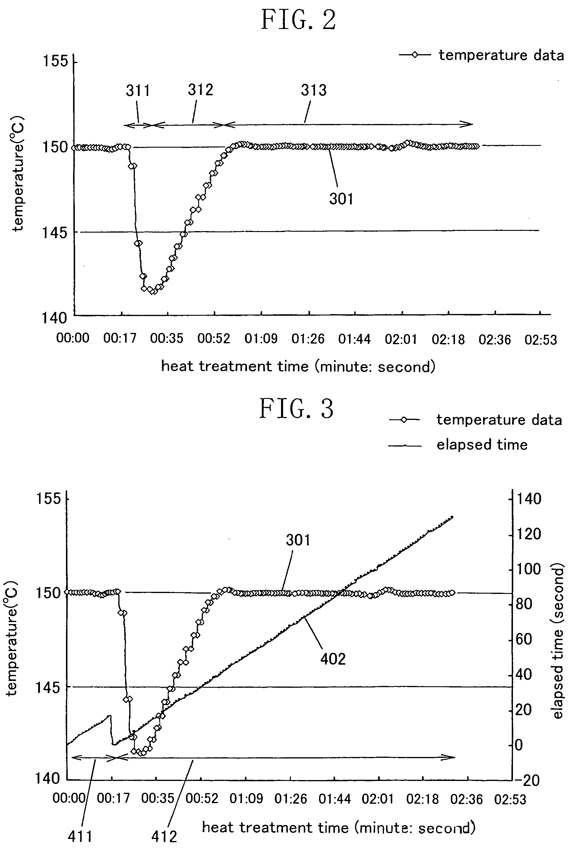
[0023] In the present invention, the management range corresponding to the parameter behavior in the transient gradient state, specifically, the management range corresponding to the temperature variation of the hot plate at placement of the article to be processed above the hot plate is calculated based on the temperature data of the hot plate, the process recipe data, and the elevation timing data for the article to be processed, and apparatus abnormality is detected with the use of the management range. Thus, detailed evaluation is enabled as to whether the temperature variation of the hot plate detected by the temperature control section in the placement of the article to be processed above the hot plate is different from the behavior of the reference temperature data (for example, temperature data measured in the past) or not. When the detected temperature variation of the hot plate is different from the behavior of the reference temperature data, for example, when the detected temperature of the hot plate does not vary so much compared with the behavior of the reference temperature data, it is judged as occurrence of apparatus abnormality, for example, abnormality that the article to be processed conveyed above the hot plate is placed at the predetermined wafer placing position inaccurately. Hence, by setting the management range per unit period for the parameter behavior showing a transient gradient, the detection, judgment, and classification of temperature abnormality in the semiconductor manufacturing apparatus can be performed more precisely than the conventional case where the “threshold value” is set for the peak value of the temperature variation of the hot plate.
[0024] As described above, the present invention relates to a method for detecting temperature abnormality in manufacturing a semiconductor device, and exhibits an effect that detection, judgment, and classification of temperature abnormality can be performed with high precision in a case applied to, for example, temperature management of a hot plate used in a photolithography process and the like, which is very effective.

Problems solved by technology

However, when it is desired to detect abnormality of a heat treatment apparatus more precisely, it is insufficient to merely set the “threshold value” for the peak value of the temperature variation of the hot plate as in the conventional technique.
In detail, the method disclosed in Patent Document 1 attains not so precise abnormality detection in a heat treatment apparatus, and it is difficult to precisely manage the apparatus.

Method used


Image

  • Temperature abnormality detection method and semiconductor manufacturing apparatus
  • Temperature abnormality detection method and semiconductor manufacturing apparatus
  • Temperature abnormality detection method and semiconductor manufacturing apparatus

Examples


Embodiment Construction

[0033] A method for detecting temperature abnormality and a semiconductor manufacturing apparatus according to one embodiment of the present invention will be descried below with reference to the accompanying drawings.

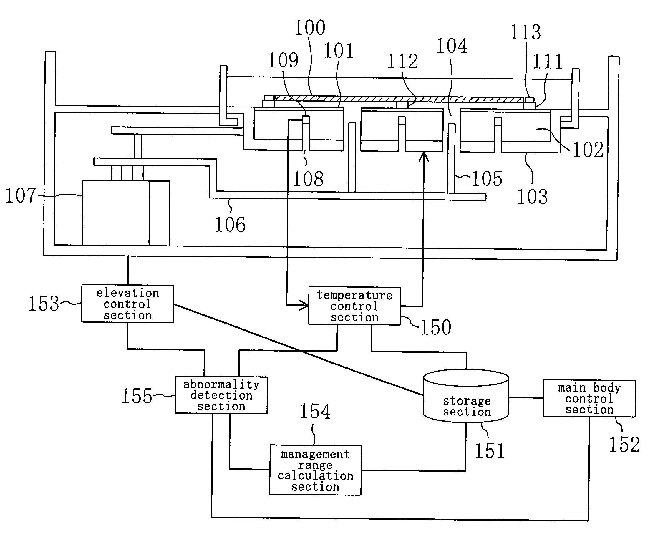
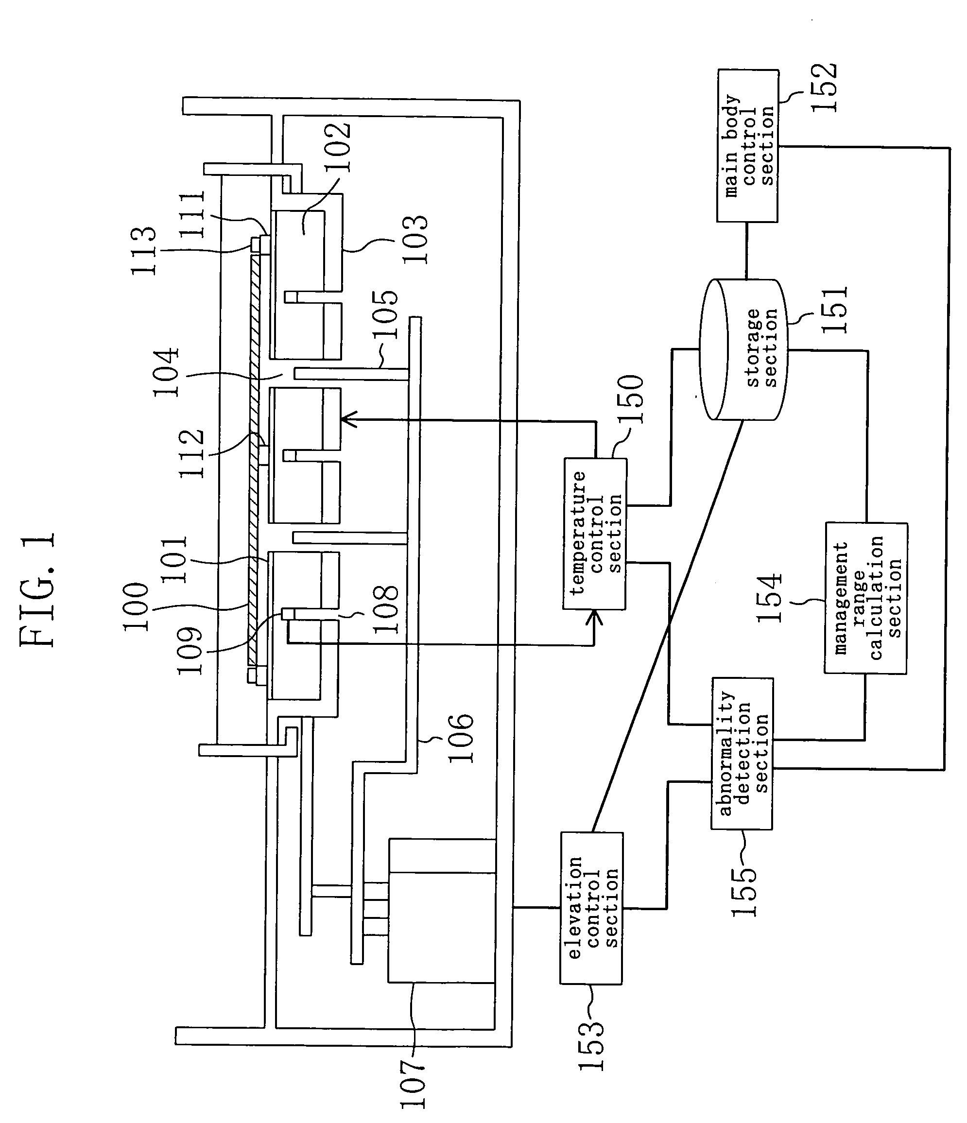
[0034]FIG. 1 is a view showing a schematic constitution of a semiconductor manufacturing apparatus (specifically, a heat treatment apparatus) according to the present embodiment. As shown in FIG. 1, a hot plate 101 as a processing plate for heat treating a wafer 100 as an article to be processed is provided at the substantial center of the heat treatment apparatus. The hot plate 101 is arranged on the obverse side of a circular holding plate 102 having a diameter, for example, slightly larger than the wafer 100. On the reverse side of the holding plate 102, a heating element 103 having, for example, substantially the same shape as that of the holding plate 102 is arranged so as to be adhered to the holding plate 102. The heating element 103 is composed of, for example...


PUM


Abstract

A semiconductor manufacturing apparatus includes: a hot plate that heats an article to be processed; a temperature control section that controls temperature of the hot plate; a main body control section that controls the entirety of the apparatus based on a process recipe; and an elevating mechanism that elevates the article to be processed above the hot plate. The semiconductor manufacturing apparatus further includes: a storage section that stores temperature data of the hot plate; an elevation control section that controls the elevating mechanism and sends elevation timing data to the storage section; a management range calculation section that calculates a management range corresponding to parameter behavior in a transient gradient state based on the temperature data, process recipe data, and the elevation timing data; and an abnormality detection section that detects apparatus abnormality with the use of the management range calculated by the management range calculation section.

Description

CROSS REFERENCE TO RELATED APPLICATIONS [0001] This Non-provisional application claims priority under 35 U.S.C. § 119(a) on Patent Application No. 2004-155832 filed in Japan on May 26, 2004, the entire contents of which are hereby incorporated by reference. FIELD OF THE INVENTION [0002] The present invention relates to a method for detecting temperature abnormality in manufacturing a semiconductor device. DESCRIPTION OF THE PRIOR ART [0003] A photolithography process for manufacturing a semiconductor device in recent years includes the steps of: a resist applying step of applying a resist on the surface of a wafer to form a resist film having uniform thickness; a pre-baking step of evaporating residual solvent in the resist film to enhance a photochemical reaction; an exposing step of transferring a device pattern to the resist on the wafer; a developing step of eluting out the exposed part of the resist film; and a post-baking step of reinforcing the resist pattern. [0004] In heat ...

Claims


Application Information

Patent Timeline
IPC IPC(8): G06F19/00H01L21/66
CPCH01L21/67248H01L22/00
Inventor SATO, NAOAKI
Owner PANASONIC CORP
Learn More