Semiconductor memory device and signal processing system

a memory device and semiconductor technology, applied in the direction of instruments, coding, code conversion, etc., can solve the problems of troublesome processing of adding redundant memory, affecting the efficiency of signal processing, and causing cost rise, so as to shorten the write time and/or read time, and make redundant memory unnecessary.

Active Publication Date: 2005-12-01
TESSERA ADVANCED TECH
View PDF6 Cites 42 Cited by
  • Summary
  • Abstract
  • Description
  • Claims
  • Application Information

AI Technical Summary

Benefits of technology

[0016] In the present invention, it is desirable to provide a semiconductor memory device able to strengthen the error correction capability, able to shorten the write time and/or read time, and...

Problems solved by technology

Consequently, the write time sometimes becomes long.
Further, since an ECC has a weak correction capability, it is necessary to form a redundant memory array other than the normal memory array.
Namely, it is necessary to perform troublesome processing of adding redundant memory is added for improving the yield at the time of the productio...

Method used


Image

  • Semiconductor memory device and signal processing system
  • Semiconductor memory device and signal processing system
  • Semiconductor memory device and signal processing system

Examples


Embodiment Construction

[0046] Below, an explanation will be given of preferred embodiments of the present invention with reference to the drawings.

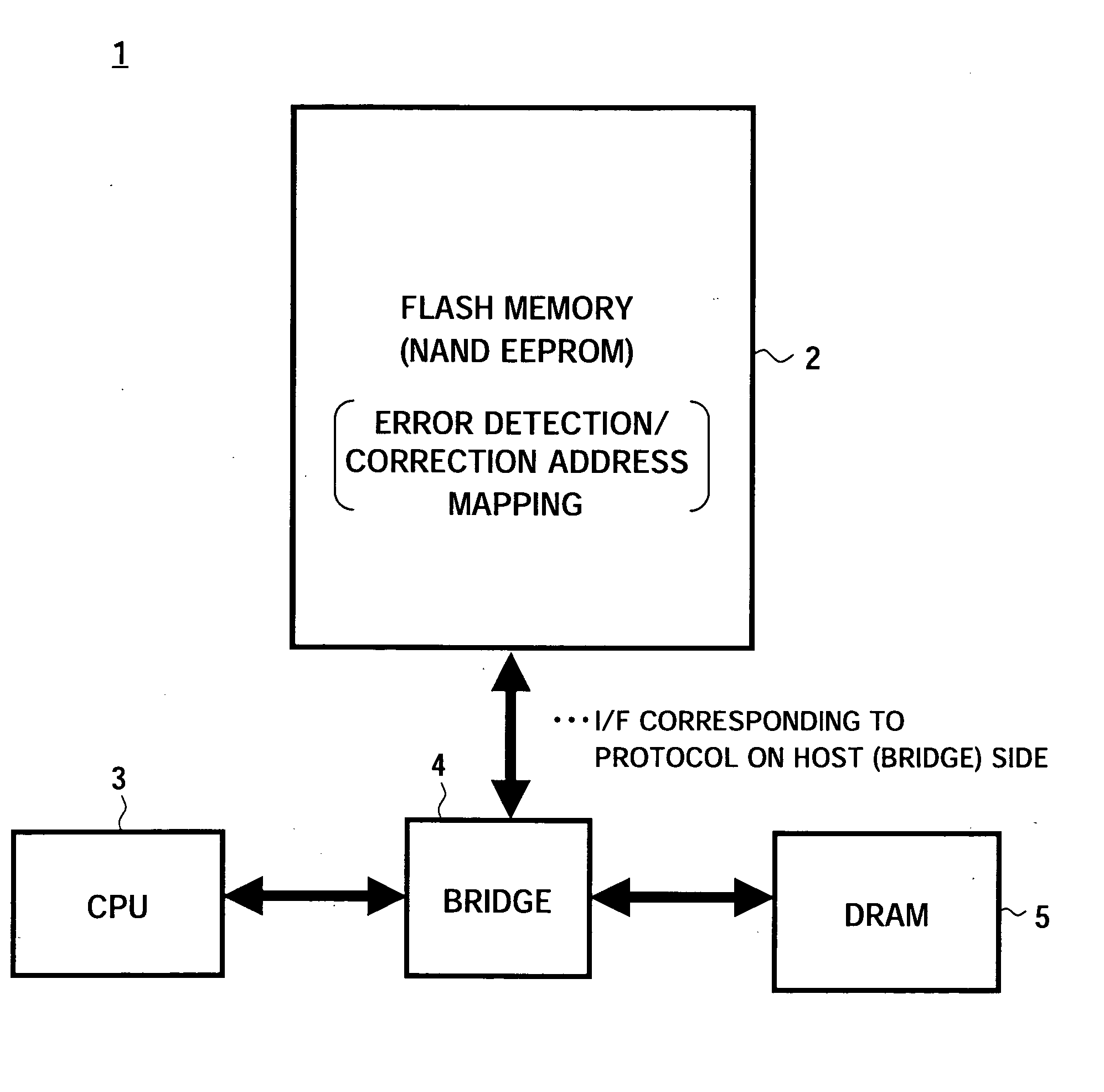
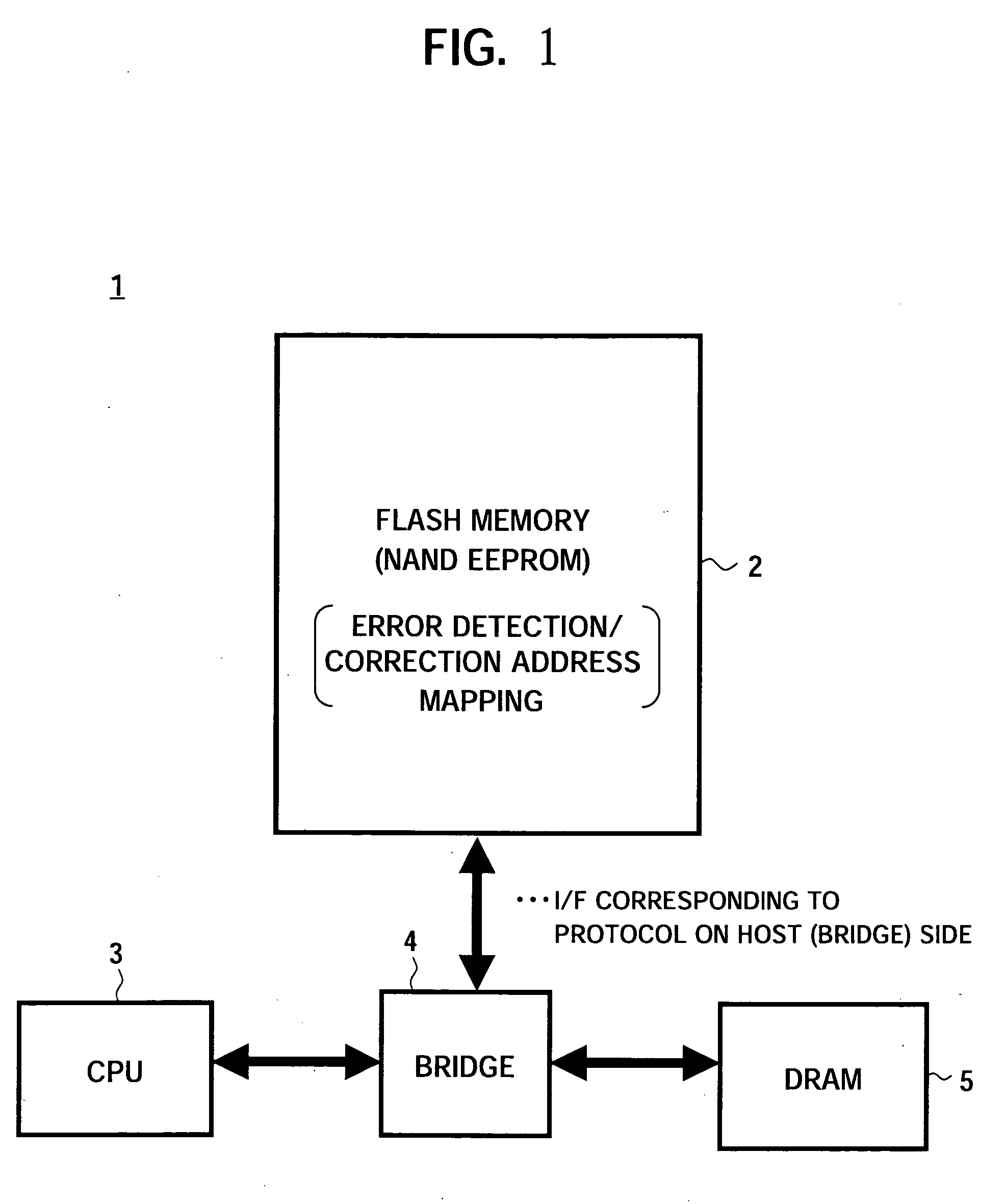
[0047]FIG. 1 is a block diagram of the overall configuration of a signal processing system employing a semiconductor memory device according to an embodiment of the present invention. In the present embodiment, as the semiconductor memory device, a NAND type flash memory in which memory strings formed by connecting pluralities of memory cells in series are connected to bit lines and source lines via selection switches is employed.

[0048] The signal processing system 1 has, as shown in FIG. 1, a NAND type flash memory 2 as a first semiconductor memory device, a central processing unit (CPU) 3 as a host device, a bridge circuit 4, and for example a dynamic random access memory (DRAM) 5 as a second semiconductor memory device.

[0049] In the signal processing system 1, the host side CPU 3 and the NAND type flash memory 2 are connected via the bridge circuit 4. Acc...


PUM


Abstract

A semiconductor memory device able to strengthen an error correction capability, able to shorten a write time and/or a read time, able to make a redundant memory unnecessary or smaller, and consequently able to achieve a reduction of size and a reduction of cost, provided with a data input portion for receiving 1 page's worth of data, dividing it to a plurality of code words, generating and adding check code (parity data), for each code word, successively forming main code words and transferring the same to a bank (A) or a bank (B), and a data output portion for receiving 1 page's worth of data including main code words transferred from the data latch circuit, correcting the error data when there is within a predetermined number of error data for each main code word, adding the error information for read each read code word except check code (parity data), and transferring the same to a host side, and a signal processing system using the same.

Description

CROSS REFERENCES TO RELATED APPLICATIONS [0001] The present invention contains subject matter related to Japanese Patent Application No. 2004-161810 filed in the Japan Patent Office on May 31, 2004 the entire contents of which being incorporated herein by reference. BACKGROUND OF THE INVENTION [0002] 1. Field of the Invention [0003] The present invention relates to a NAND type flash memory or other semiconductor memory device having memory strings connected to bit lines and source lines via selection switches and to a signal processing system provided with such a semiconductor memory device, more particularly relates to an error correction processing technology of a semiconductor memory device. [0004] 2. Description of the Related Art [0005] In a NAND type flash memory, a plurality of memory transistors are connected in series to form memory strings. Two memory strings share one bit contact and source line, whereby a higher integration is achieved. [0006] In a general NAND type flas...

Claims


Application Information

Patent Timeline
IPC IPC(8): G11C16/02G06F11/10G11C16/06G11C29/00H03M13/00
CPCG06F11/1068G11C16/00
Inventor SHIMIZUME, KAZUTOSHIAKITA, MAMORUITOH, MASAHIKO
Owner TESSERA ADVANCED TECH
Why Eureka
Try Eureka