Negative differential resistance pull up element for DRAM

a pull-up element and differential resistance technology, applied in the field of dynamic random access memory cells, can solve the problems of inability to operate, diode type structures, limited ndr devices to two terminals, etc., and achieve the effect of convenient integration

Inactive Publication Date: 2005-12-08
SYNOPSYS INC
View PDF90 Cites 41 Cited by
  • Summary
  • Abstract
  • Description
  • Claims
  • Application Information

AI Technical Summary

Benefits of technology

[0012] Yet another object of the present invention is to provide an improved type of NDR device that is more flexible and more easily integrated (than prior NDR diode devices) into conven...

Problems solved by technology

To date, such NDR devices have been limited to two terminal, diode type structures which have operational limitations as well as integration complexities with CMOS processing.
Furthermore, it is ...

Method used


Image

  • Negative differential resistance pull up element for DRAM
  • Negative differential resistance pull up element for DRAM
  • Negative differential resistance pull up element for DRAM

Examples


Embodiment Construction

[0033] The following detailed description is meant to be illustrative only of particular embodiments of the invention. Other embodiments of the invention and variations of those disclosed will be obvious to those skilled in the art in view of the following description.

[0034] As discussed below, a preferred device embodiment is described first. Next, the mechanism responsible for the negative differential resistance (NDR) mode is described, followed by additional preferred embodiments for enhancing the performance of an NDR device. Finally, an exemplary method of fabrication will be described.

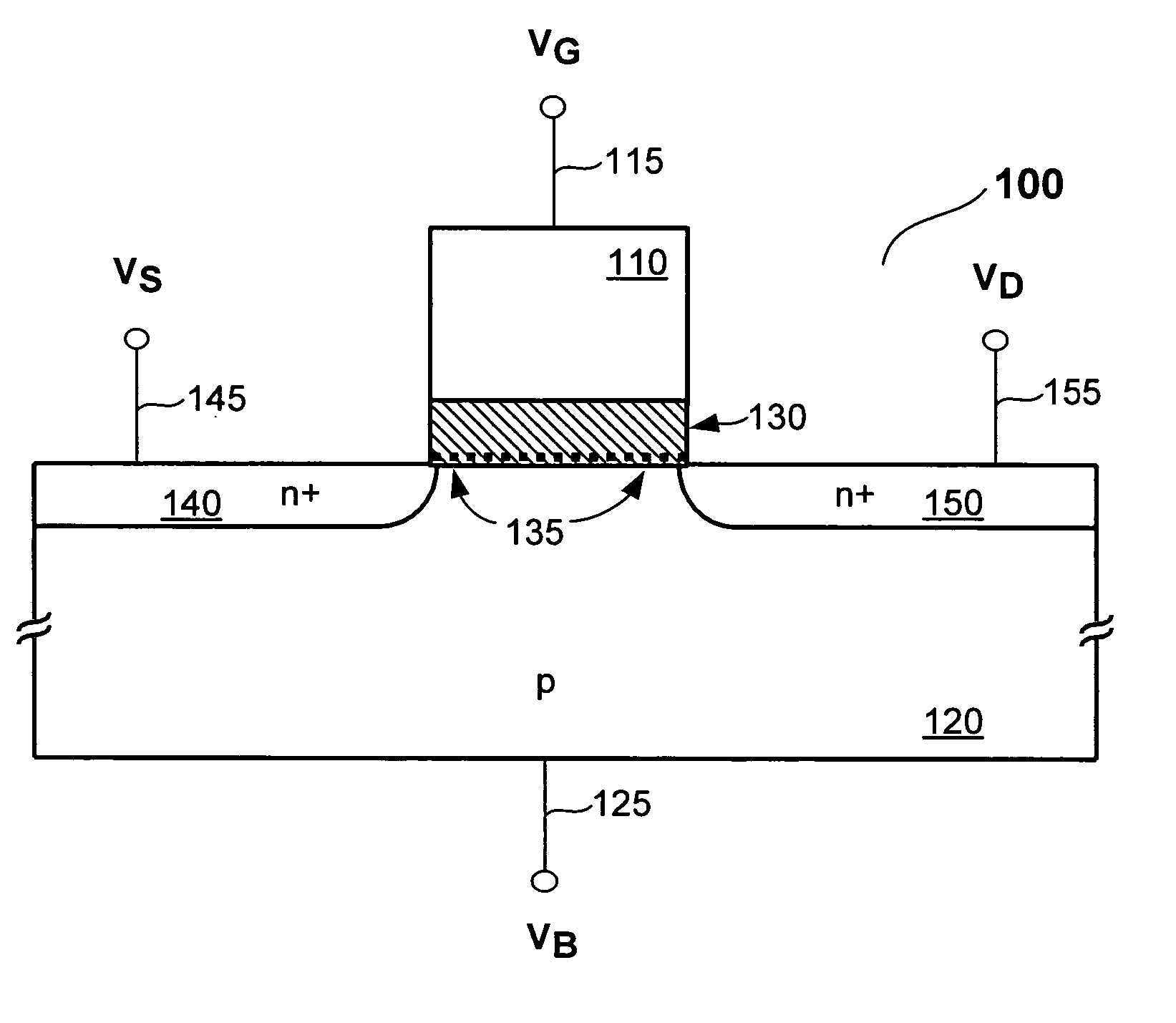
[0035] In accordance with a preferred embodiment of the invention, an n-channel field effect transistor (FET) NDR device structure (FIG. 1) 100 is provided which is made with minimum modification to a standard CMOS process. In fact, from a first glance, device 100 appears to be an ordinary n-channel MOS (NMOS) transistor, in which a gate electrode 110 of the device is formed on top of a semico...


PUM


Abstract

A memory cell includes a pull-up element that exhibits a refresh behavior that is dependent on the data value stored in the memory cell. The pull-up element is an NDR FET connected between a high voltage source and a storage node of the memory cell. The NDR FET receives a pulsed gate bias signal, wherein each pulse turns on the NDR FET when a logic HIGH value is stored at the storage node, and further wherein each pulse does not turn on the NDR FET when a logic LOW value is stored at the storage node. In this fashion a DRAM cell (and device) can be operated without a separate refresh cycle.

Description

CROSS REFERENCE TO RELATED APPLICATIONS [0001] The present application is a continuation-in-part of Ser. No. 10 / 828,356 entitled CHARGE TRAPPING PULL-UP ELEMENT filed Apr. 19, 2004 which is a divisional of Ser. No. 10 / 298,916 entitled FIELD EFFECT TRANSISTOR PULL-UP / LOAD ELEMENT filed Nov. 18, 2002 (U.S. Pat. No. 6,724,024) which is a continuation of Ser. No. 10 / 028,085 entitled NEGATIVE DIFFERENTIAL RESISTANCE FIELD EFFECT TRANSISTOR (NDR-FET) AND CIRUITS USING THE SAME filed Dec. 21, 2001 (U.S. Pat. No. 6,559,470).FIELD OF THE INVENTION [0002] This invention relates to semiconductor devices and more particularly to a dynamic random access memory cell that uses a negative differential resistance (NDR) pull-up element. BACKGROUND OF THE INVENTION [0003] A new type of CMOS compatible, NDR capable FET is described in the aforementioned application King referenced above. The advantages of such device are well set out in such materials, and are not repeated here. [0004] In preferred emb...

Claims


Application Information

Patent Timeline
IPC IPC(8): G11C11/405G11C11/406H01L21/8242H01L27/105H01L27/108H01L27/11H01L29/423H01L29/76H01L29/788H01L29/792
CPCB82Y10/00G11C11/405G11C11/406G11C11/40615G11C2211/4016H01L27/105H01L29/792H01L27/10873H01L27/1112H01L29/42324H01L29/78H01L29/788H01L29/7881H01L27/108H10B12/00H10B12/05H10B10/15
Inventor KING, TSU-JAE
Owner SYNOPSYS INC
Why Eureka
Try Eureka