Light source device and projector

a light source device and projector technology, applied in the field of light source devices and projectors, can solve the problems of low thermal conductivity of organic adhesives that are generally used as fillers, inability to effectively conduct heat, and limitation of cross-sectional area of solder balls, so as to achieve high thermal conductivity and improve thermal conduction efficiency

Inactive Publication Date: 2005-12-08
SEIKO EPSON CORP
View PDF4 Cites 12 Cited by
  • Summary
  • Abstract
  • Description
  • Claims
  • Application Information

AI Technical Summary

Benefits of technology

[0010] In this case, since a filling agent with an excellent thermal conductivity lies between the light-emitting element and the support member, heat generated from the light-emitting element is efficiently conducted to the support member that is a mounting substrate. Accordingly, when it is used as a light source light, a light source device that is not likely to over-heat, and has sufficient and stable emission brightness can be obtained.
[0012] As another more specific mode involving the invention, the insulating material includes solid particles that have a thermal conductivity larger than that of air. In this case, when the solid particles with a larger thermal conductivity are selected, it becomes possible to carry out more effective thermal conduction. Accordingly, a cooling effect of the light-emitting element can be improved.
[0016] Furthermore, as a further specific mode involving the invention, the electrically conductive material includes solid particles having electrical conductivity. In this case, it is possible to choose solid particles with desired electrical conductivity and, in general, the electrically conductive substance has high thermal conductivity. Accordingly, it is possible to further improve the thermal conduction efficiency.

Problems solved by technology

However, organic adhesives that are generally used as filler are so low in the thermal conductivity that heat cannot be effectively conducted, and in addition to this, there is a limitation in a cross-sectional area of a solder ball that forms a flip chip.

Method used


Image

  • Light source device and projector
  • Light source device and projector
  • Light source device and projector

Examples


first embodiment

THE FIRST EMBODIMENT

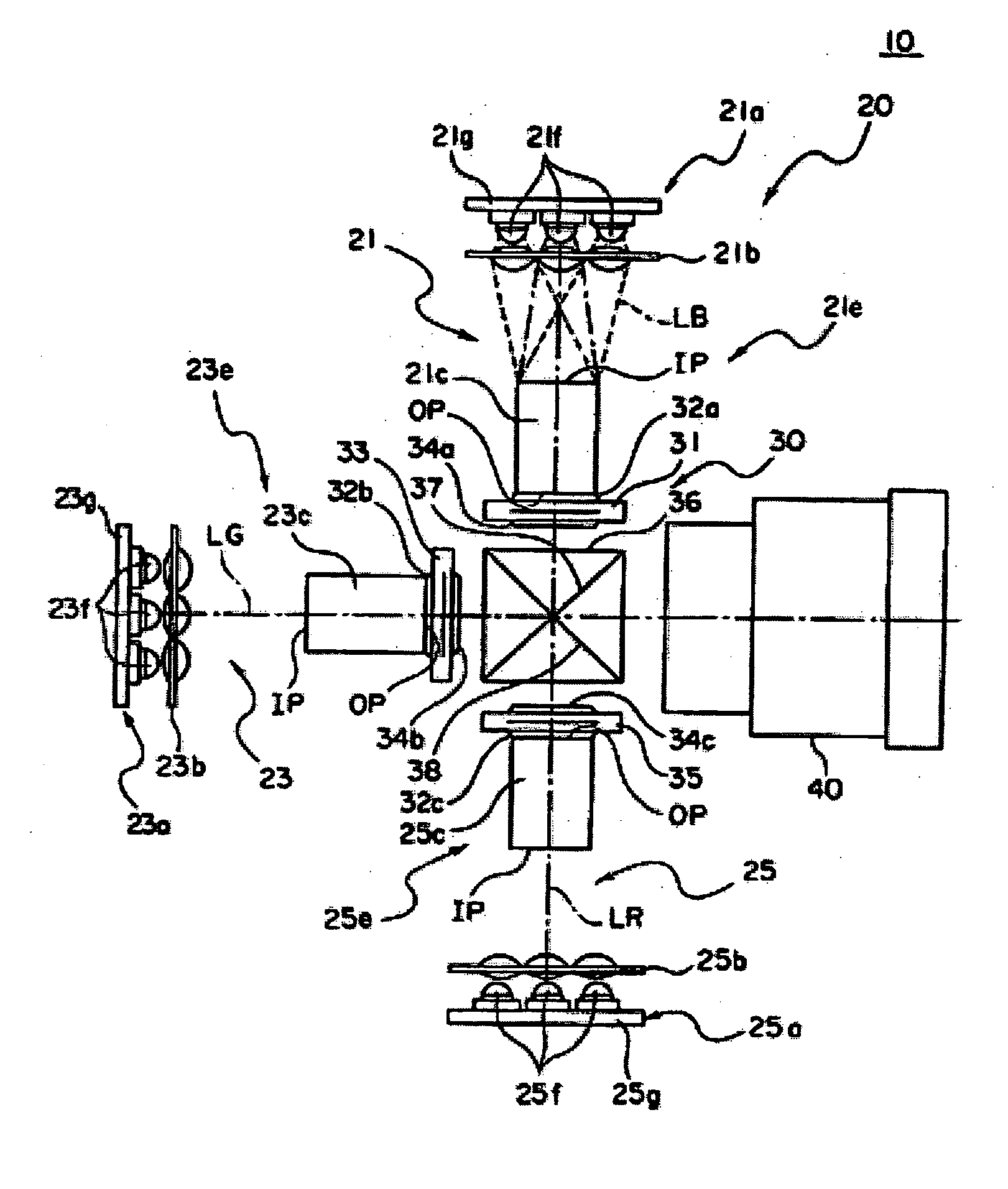
[0028]FIG. 1 is a block diagram of a projector 10 that has a light source device involving the invention. The projector 10 has a light source device 20, an image formation unit 30, and a projection lens 40. Here, the light source device 20 has a blue light source device 21, a green light source device 23, and a red light source device 25. The image formation unit 30 has polarizing filters 32a, 32b, 32c, 34a, 34b, and 34c that control a direction of polarization; three liquid crystal light bulbs 31, 33, and 35 that are light transmissive light modulators; and a cross dichroic prism 36 that is a light synthesizing member.

[0029] The blue light source device 21 has a blue light source unit 21a and an illuminating light formation optical system 21e. Among these, the blue light source unit 21a is manufactured by mounting a plurality of LED packages 21f that are electronic parts each incorporating an LED that is a solid light-emitting element on a circuit board 21g tha...

second embodiment

THE SECOND EMBODIMENT

[0042] In the first embodiment, an insulating material is used as a material for a filling material FL. However, in the present embodiment, a case where an electrically conductive material is used, and furthermore, an insulating member is used to insulate between the electrodes will be considered.

[0043] In the case where the light source device in the embodiment is applied to each of the projectors shown in FIGS. 1 and 3, except for a mounting method of the package, a structure which is the same as that in the first embodiment can be used. Accordingly, the explanation will be omitted except for portions relating to a mounting method.

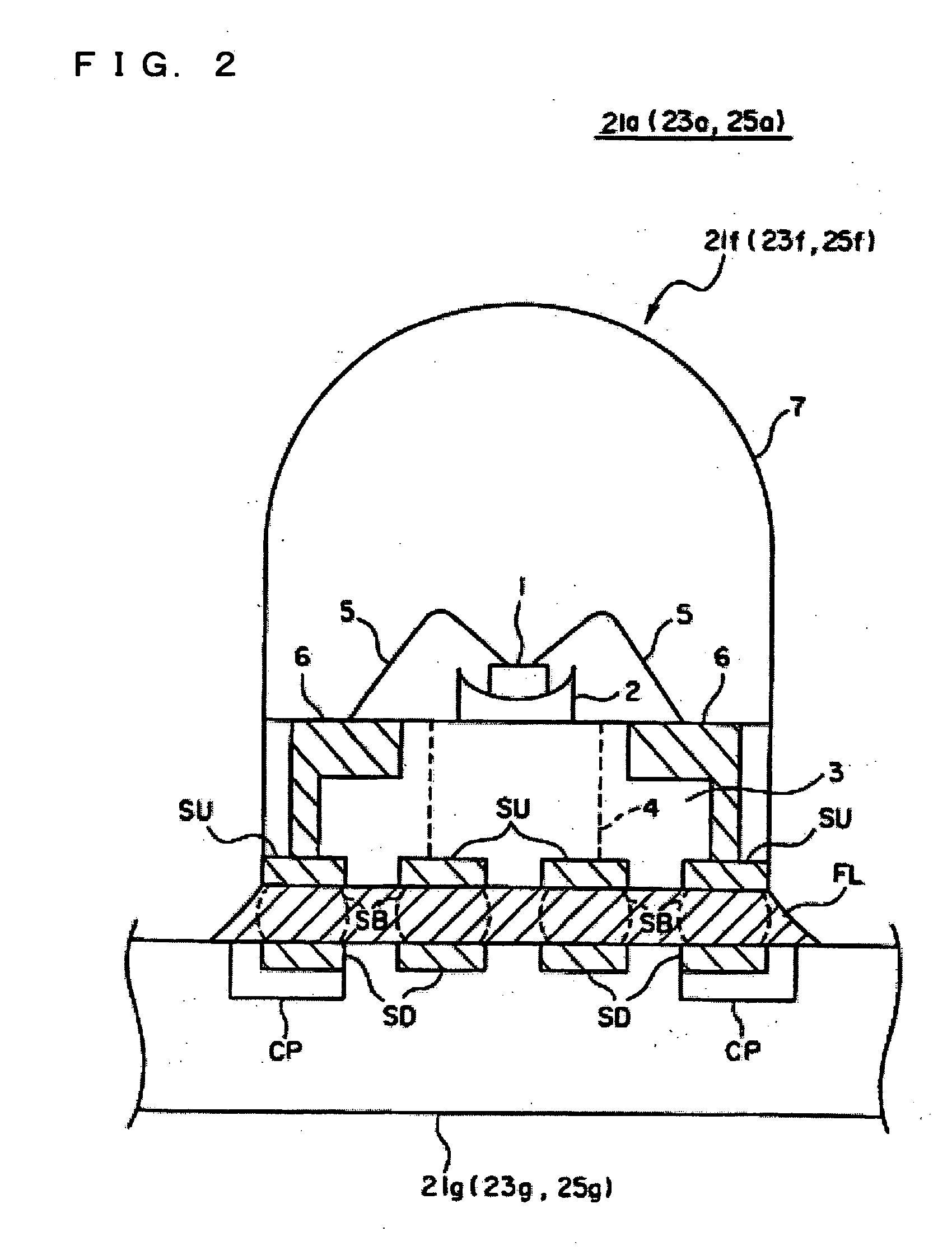
[0044]FIG. 4 is an expanded sectional view for explaining, in each of the light source units 21a (23a, 25a and 120a) in the embodiment, a structure of the LED package 21f (23f, 25f and 120f) and a state where the LED package 21f (23f, 25f and 120f) is mounted on the circuit board 21g (23g, 25g and 120g). Here, the LED package 21f t...


PUM


Abstract

A light source device is provided comprising: a light-emitting element; a support member having the light-emitting element flip chip mounted thereto; and a thermally conductive filling agent between the light-emitting element and the support member. By injecting the filling agent between the light-emitting element and the support member, the thermal conduction is supplemented by the filling agent. As such, heat generated by the light-emitting element can be efficiently removed outside the light source device.

Description

RELATED APPLICATIONS [0001] This application claims priority to Japanese Patent Application No. 2004-164497 filed Jun. 2, 2004 which is hereby expressly incorporated by reference herein in its entirety. BACKGROUND [0002] 1. Technical Field [0003] The present invention relates to a light source device with a light-emitting element such as a light-emitting diode functioning as a light source and formed on a substrate by a mounting technique including a flip chip technique and so on, and a projector therewith. [0004] 2. Related Art [0005] A known technique for attaching an LED (light-emitting diode) chip like a flip chip uses ultrasonic welding and a metal bump (JP-A No. 2003-8071). [0006] Furthermore, in flip-chip mounting of a semiconductor chip and so on, in order to avoid damaging a solder joint due to thermal stress caused by a difference in the thermal expansion coefficients, it is known to fill a sealing resin containing filler between continuation and connection solder balls (J...

Claims


Application Information

Patent Timeline
Patent Type & Authority Applications(United States)
IPC IPC(8): G03B21/00G03B21/20H01L33/60H01L33/62H01L33/64
CPCH01L33/62H01L2224/48091H04N9/3144H04N9/315Y10S362/80H01L2924/12041G03B21/2033H01L2924/00014
Inventor NAKAMURA, NORIO
Owner SEIKO EPSON CORP
Why Eureka
Try Eureka