Optical disk device and program for recording and reproducing information on and from an optical recording medium

a technology of optical disk and program, which is applied in the direction of digital signal error detection/correction, instruments, recording signal processing, etc., can solve the problems of inability of drive manufactures to prepare strategies appropriate for all optical disks on the market, not necessarily an optimal write strategy for an optical disk in use, and failure to mark forming, etc., to achieve the effect of reducing useless processing tim

Inactive Publication Date: 2005-12-08
SAMSUNG ELECTRONICS CO LTD
View PDF4 Cites 16 Cited by
  • Summary
  • Abstract
  • Description
  • Claims
  • Application Information

AI Technical Summary

Benefits of technology

[0028] In accordance with the above-described inventions, the calculation determination means can determine whether to calculate the jitter value using the jitter value calculation unit based on the ratio of the average values and the standard deviations. That is, when th...

Problems solved by technology

A difference in the composition of a dye recording layer constituting the optical disk causes a failure in mark forming resulting from the heat accumulation of the recording medium or insufficient cooling speed.
Since there are so many types of commercialized optical disks that drive manufacturers cannot know them all, it is impossible for the drive manufactures to prepare strategies appropriate for all the optical disks on the market.
However, in the former method, a finally selected write strategy is merely the b...

Method used


Image

  • Optical disk device and program for recording and reproducing information on and from an optical recording medium
  • Optical disk device and program for recording and reproducing information on and from an optical recording medium
  • Optical disk device and program for recording and reproducing information on and from an optical recording medium

Examples


Embodiment Construction

[0046] Reference now should be made to the drawings, in which the same reference numerals are used throughout the different drawings to designate the same or similar components.

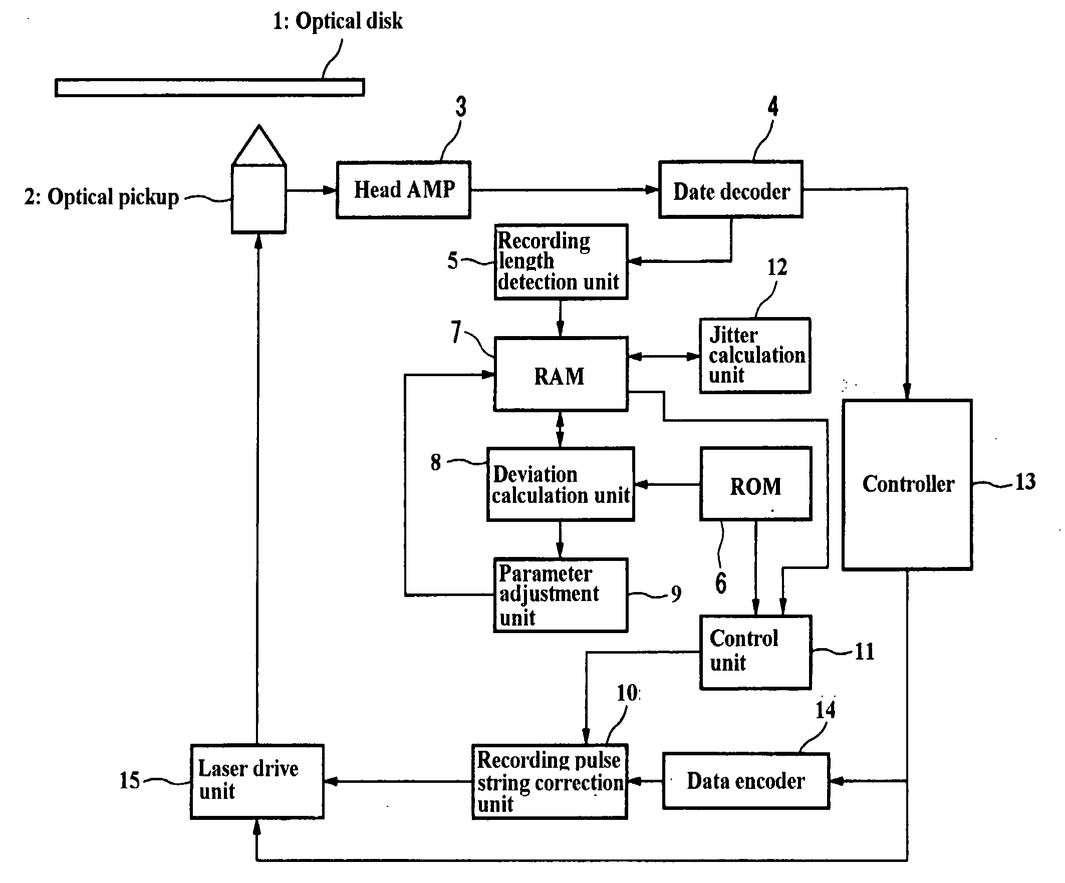
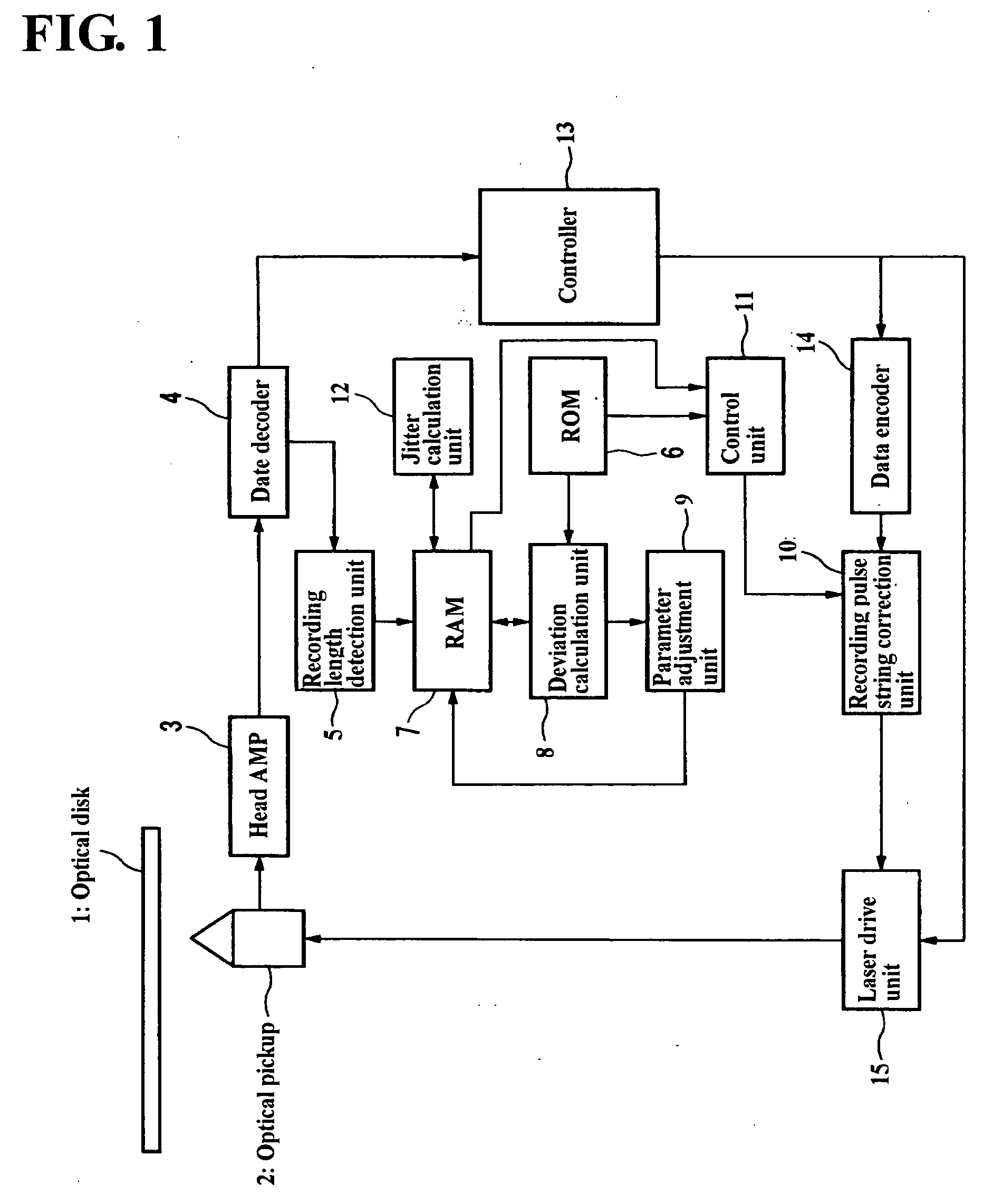
[0047] An optical disk device according to the present embodiment, as shown in FIG. 1, includes an optical disk 1, an optical pickup 2, a head amplifier 3, a data decoder 4, a recording length detection unit 5, Read-Only Memory (ROM) 6, RAM 7, a deviation calculation unit 8, a parameter adjustment unit 9, a recording pulse string correction unit 10, a control unit 11, a jitter calculation unit 12, a controller 13, a data encoder 14, and a laser drive unit 15.

[0048] The optical disk 1 is an optical information recording medium for recording, reproducing and erasing information using a semiconductor laser. The optical disk 1 may be, for example, a CD-R, a CD-RW, a DVD-R, a DVD-RW or a DVD-RAM.

[0049] The optical pickup 2 includes a laser light source, such as a laser diode (not shown), optical parts, such as ...


PUM

PropertyMeasurementUnit
Lengthaaaaaaaaaa
Flexibilityaaaaaaaaaa

Abstract

The present invention relates to an optical disk device for recording or reproducing information on or from an optical information recording medium by forming marks and spaces. The device includes a jitter value measurement unit, a measurement unit, measured value memory, theoretical length memory, a deviation value calculation unit, a flexibility amount calculation unit, a correction value calculation unit, and a jitter value calculation unit. The measurement unit measures the lengths of marks and spaces using a varied reference write strategy. The deviation value calculation unit calculates the deviation values of the marks and the spaces. The flexibility amount calculation unit calculates the amounts of intrinsic flexibility of all marks and spaces. The correction value calculation unit calculates a correction value for the reference write strategy. The jitter value calculation unit calculates a jitter value.

Description

INCORPORATION BY REFERENCE [0001] The present application claims priority under 35 U.S.C. §119 to Japan Patent Application No. 2004-150501 filed on May 20, 2004. The content of the application is incorporated herein by reference in its entirety. BACKGROUND OF THE INVENTION [0002] 1. Field of the Invention [0003] The present invention relates generally to an optical disk device and program for recording and reproducing information on and from an optical recording medium such as a compact disk and a digital video disk. [0004] 2. Description of the Related Art [0005] As the Internet has remarkably become popularized due to the advance of information and communication technology, much information is actively being exchanged over a network. Under this environment, in the field of information recording device technology, a write-once read-many optical disk, such as a Compact Disk-Recordable (CD-R), or a rewritable optical disk, such as a Compact Disk-Rewritable (CD-RW), is recently attrac...

Claims


Application Information

Patent Timeline
IPC IPC(8): G11B7/0045G11B7/00G11B7/125G11B5/09
CPCG11B7/00456G11B7/1267B65D83/0882B65H35/002B65H35/0086B65H2301/5151B65H2301/51532B65H2301/5154B65H2701/1944
Inventor NAKAJO, YUKIHISA
Owner SAMSUNG ELECTRONICS CO LTD
Why Eureka
Try Eureka