Process for ultra-thin body SOI devices that incorporate EPI silicon tips and article made thereby

a technology of epi silicon tips and fabrication process, applied in the direction of semiconductor devices, electrical devices, transistors, etc., can solve problems such as critical dimensions

Inactive Publication Date: 2005-12-08
INTEL CORP
View PDF46 Cites 28 Cited by
  • Summary
  • Abstract
  • Description
  • Claims
  • Application Information

AI Technical Summary

Problems solved by technology

One challenge for ULSI is that more transistors must be incorporated into an integrated circuit (IC), while attempting to decrease the overall size of the semiconductive substrate.
One challenge is that photolithographic techniques cause a critical dimension to be the smallest feature patternable.
Other challenges include proper electrical isolation between adjacent devices in the face of the relentless pressure to crowd devices closer to each other.

Method used


Image

  • Process for ultra-thin body SOI devices that incorporate EPI silicon tips and article made thereby
  • Process for ultra-thin body SOI devices that incorporate EPI silicon tips and article made thereby
  • Process for ultra-thin body SOI devices that incorporate EPI silicon tips and article made thereby

Examples


Embodiment Construction

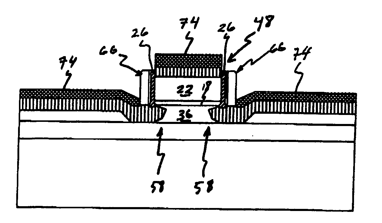
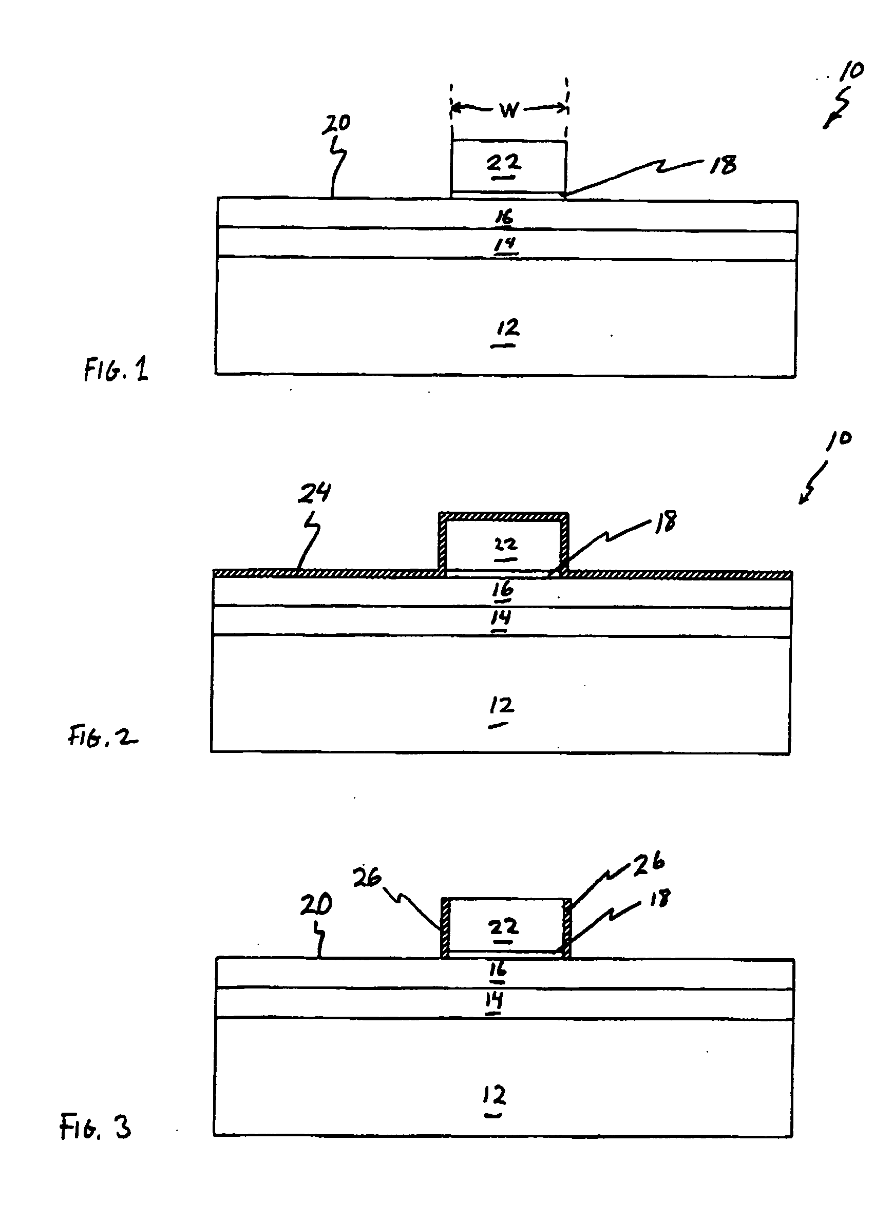
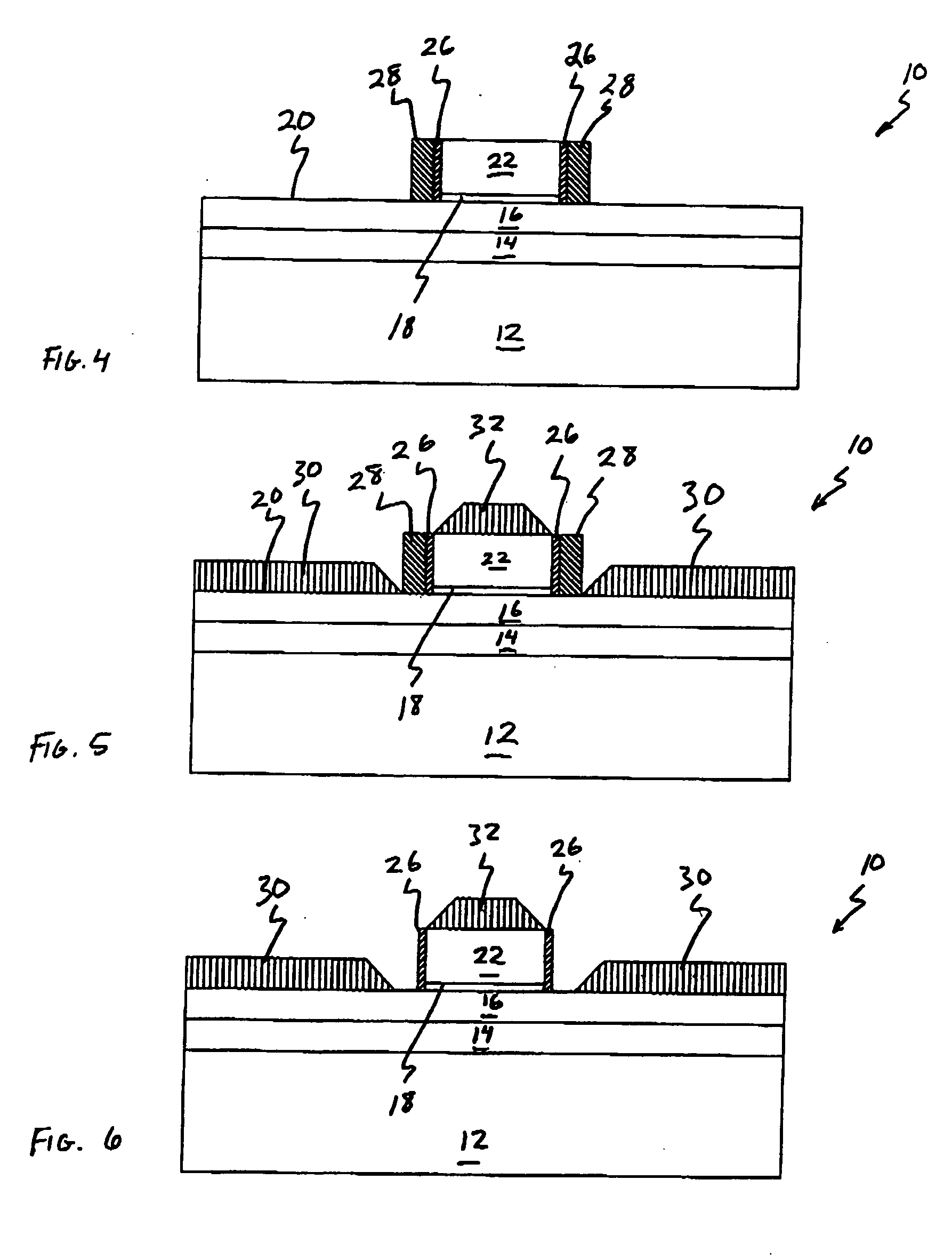
[0023] The present invention relates a process flow that forms an ultra-thin body silicon-on-insulator (SOI) transistor. FIG. 1 is an elevational cross section that illustrates a semiconductor device 10 during fabrication. Semiconductor device 10 includes a substrate 12 that by way of non-limiting example, is a p-type metal oxide semiconductor device (PMOS) or an n-type metal oxide semiconductor device (NMOS). According to the present invention, one embodiment of substrate 12 includes an SOI configuration. Accordingly, substrate 12 has an SOI insulator layer 14, and an SOI silicon layer 16. The formation of the SOI configuration is carried out according to known technique. Although an SOI configuration is depicted, other isolation structures may be added such as local isolation of silicon (LOCOS), recessed LOCOS, or shallow trench isolation (STI).

[0024] A gate dielectric layer 18 is formed on the upper surface 20 of substrate 12 as shown in FIG. 1. In one embodiment, gate dielectri...


PUM


Abstract

The invention relates to a transistor that includes an ultra-thin body epitaxial layer that forms an embedded junction with a channel that has a length dictated by an undercut under the gate stack for the transistor. The invention also relates to a process of forming the transistor and to a system that incorporates the transistor.

Description

FIELD OF THE INVENTION [0001] An embodiment of the present invention relates generally to integrated circuit fabrication. More particularly, an embodiment of the present invention relates to a method of fabricating an ultra-thin body silicon on oxide (SOI) device. BACKGROUND OF THE INVENTION DESCRIPTION OF RELATED ART [0002] Transistor technology has progressed to include large-scale integration (LSI), very large-scale integration (VLSI), and ultra large-scale integration (ULSI), with further improvements appearing on the technical horizon. One challenge for ULSI is that more transistors must be incorporated into an integrated circuit (IC), while attempting to decrease the overall size of the semiconductive substrate. One requirement is that the semiconductive channel length is preferably shortened in order to further assist the miniaturization process. One challenge is that photolithographic techniques cause a critical dimension to be the smallest feature patternable. For example, ...

Claims


Application Information

Patent Timeline
Patent Type & Authority Applications(United States)
IPC IPC(8): H01L21/336H01L29/417H01L29/786
CPCH01L29/41733H01L29/665H01L29/6656H01L29/66636H01L29/66772H01L29/78618
Inventor MURTHY, ANANDDOYLE, BRIANKAVALIEROS, JACKCHAU, ROBERT
Owner INTEL CORP
Why Eureka
Try Eureka