Dual damascene integration structure and method for forming improved dual damascene integration structure

a technology of integration structure and damascene, applied in the direction of basic electric elements, electrical equipment, electric discharge tubes, etc., can solve the problems of substantial impact effects of large cluster ions, achieve better control of etched trench depth and shape, reduce the susceptibility of contamination, and improve the effect of interconnection resistance and capacitan

Inactive Publication Date: 2005-12-08
TEL EPION
View PDF26 Cites 40 Cited by
  • Summary
  • Abstract
  • Description
  • Claims
  • Application Information

AI Technical Summary

Benefits of technology

[0026] It is an objective of this invention to provide methods of GCIB processing of low-k dielectric materials to form dual damascene integration structures that minimize the requirement to use hard-masks.
[0028] It is a further objective of this invention to provide methods of densifying and sealing all etched surfaces to reduce their susceptibility to contamination from subsequent processes.
[0029] It is a still further objective of this invention to provide better control over etched trench depths and shapes and resultant interconnection resistance and capacitance.

Problems solved by technology

Consequently, the impact effects of large cluster ions are substantial, but are limited to a very shallow surface region.

Method used


Image

  • Dual damascene integration structure and method for forming improved dual damascene integration structure
  • Dual damascene integration structure and method for forming improved dual damascene integration structure
  • Dual damascene integration structure and method for forming improved dual damascene integration structure

Examples


first embodiment

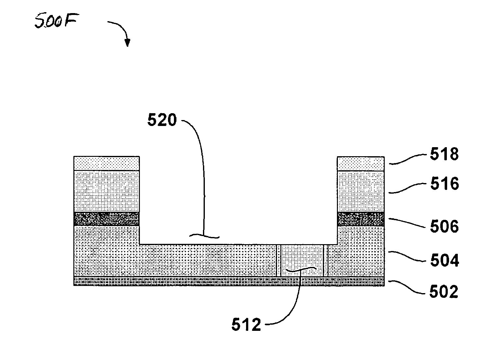
[0048]FIGS. 4A-4G illustrate in-process integration structures 500A-500G resulting from inventive process steps in the present invention, a method for fabricating the dual damascene integration structure 500H shown in FIG. 4H incorporating porous ULK dielectrics. None of the suggested dimensions in any of the following embodiments are intended to limit the invention in any manner to such embodiments.

[0049] Referring to FIG. 4A, a process in accordance with the first embodiment of the invention begins with deposition of a sequence of insulator films over the previous metal wiring level (not shown, but would appear below the stop film layer 502 in structure 500A.) The insulator stack is comprised of an etch stop film 502, porous ULK dielectric layer 504 and a hard-mask layer 506. The etch stop material has the same requirements as previously stated for the prior art processes and therefore is typically composed of a material such as Si3N4 or SiCN. The etch stop film 502 may have a thi...

second embodiment

[0058]FIGS. 5A-5G illustrate in-process structures 600A-600F and a final dual damascene integration structure 600G using porous ULK dielectrics, formed in accordance with the present invention, and which is based on initial transfer of a trench pattern into a hard-mask.

[0059] As shown in FIG. 5A, the process of the second embodiment begins with deposition of a sequence of insulator films over the previous metal wiring level. This insulator stack 600A is comprised of an etch stop film 602, a porous ULK dielectric layer 604 and a hard-mask layer 606. A masking material layer comprised of an optional antireflective coating 608 and photoresist layer 610 are then applied to this insulator stack as also illustrated in this figure. The etch stop material has the same requirements as previously stated for the prior art processes and therefore is typically a material such as Si3N4 or SiCN. The etch stop film 602 may have a thickness (for example) of about 35 nm. The porous ULK dielectric lay...


PUM

PropertyMeasurementUnit
angle of beam incidenceaaaaaaaaaa
thicknessesaaaaaaaaaa

Abstract

Methods for forming a dual damascene dielectric structure in a porous ultra-low-k (ULK) dielectric material by using gas-cluster ion-beam processing are disclosed. These methods minimize hard-mask layers during dual damascene ULK processing and eliminate hard-masks in the final ULK dual damascene structure. Methods for gas-cluster ion-beam etching, densification, pore sealing and ashing are described that allow simultaneous removal of material and densification of the ULK interfaces. A novel ULK dual damascene structure is disclosed with densified interfaces and no hard-masks.

Description

CROSS-REFERENCE TO RELATED APPLICATIONS [0001] This application claims the benefit of priority to, and incorporates herein by reference, U.S. provisional patent application Ser. No. 60 / 576,439, filed Jun. 3, 2004, and entitled “Improved Dual Damascene Integration Structure and Method for Forming Improved Dual Damascene Integration Structure.”FIELD OF THE INVENTION [0002] This invention relates generally to improved dual damascene integration structures for semiconductor integrated circuits utilizing low dielectric constant (low-k) dielectrics, and to methods of forming such structures using low-k dielectrics and the application of gas-cluster ion-beam processing. BACKGROUND OF THE INVENTION [0003] The semiconductor industry has had tremendous success in delivering ever more cost effective chips to market through the use of scaling. However, while scaling works well in device or front end of semiconductor processing, device wiring is not amenable to scaling and results in degraded in...

Claims


Application Information

Patent Timeline
Patent Type & Authority Applications(United States)
IPC IPC(8): H01L21/26H01L21/302H01L21/306H01L21/3105H01L21/311H01L21/324H01L21/42H01L21/44H01L21/477H01L21/768
CPCH01J2237/0812H01L21/02046H01L21/3105H01L21/31116H01L21/31138H01L21/31144H01L21/76807H01L21/76808H01L21/76814H01L21/7682H01L21/76825H01L21/76831
Inventor GEFFKEN, ROBERT M.HAUTALA, JOHN J.
Owner TEL EPION
Why Eureka
Try Eureka