Low voltage differential amplifier circuit for wide voltage range operation

a technology of low voltage and amplifier circuit, which is applied in the direction of dc-amplifiers with dc-coupled stages, different amplifiers, amplifiers with semiconductor devices/discharge tubes, etc., can solve the problem that the ideal operating characteristics of such conventional circuit designs cannot be achieved, and achieve the effect of wide range of input levels, improved performance and improved signal rang

Active Publication Date: 2005-12-15
PROMOS TECH INC
View PDF8 Cites 5 Cited by
  • Summary
  • Abstract
  • Description
  • Claims
  • Application Information

AI Technical Summary

Benefits of technology

[0003] In accordance with the present invention, a low voltage differential amplifier circuit and bias control techniques are disclosed which enable the accommodation of an increased range of input signals. In a particular embodiment thereof, the invention disclosed is a differential amplifier which provides substantially symmetrical voltage transitions at an output thereof in response to differential input signals supplied thereto. The amplifier comprises a current mirror coupled to a supply voltage source, a differential pair for receiving the differential input signals coupled to the current mirror and defining the output therebetween, a current source for coupling the differential pair to a reference voltage source and a current path coupled between the current mirror and the reference voltage source.
[0004] In another embodiment thereof, the invention disclosed provides a differential amplifier which comprises a current mirror comprising first and second transistors having first, second and control terminals thereof with the current mirror being coupled to a supply voltage source. A differential pair comprising third and fourth transistors having first, second, control and substrate terminals thereof is coupled to the current mirror. A current source comprising a fifth transistor having first, second and control terminals thereof is coupled to the differential pair and a reference voltage source and a control circuit is coupled to the substrate terminals of the third and fourth transistors for controlling their threshold voltage.
[0005] Particularly disclosed herein is a differential amplifier of especial applicability for low voltage operation that controls the threshold voltage of n-channel differential input transistors using substrate bias in order to allow a wider range of the input levels. Still further disclosed herein is a differential amplifier of especial applicability for low voltage operation in which an additional bias current is introduced that enables the output pull-up current to be increased without increasing the pull-down current.
[0006] In a further embodiment thereof, the invention disclosed provides a method for generating and controlling the substrate bias of a differential amplifier comprising a differential amplifier identical to the differential amplifier whose substrate bias is to be controlled. One input of said identical amplifier is set to a fixed bias and the other input is connected to one of the inputs of the differential amplifier whose substrate bias is to be controlled. The output of said identical differential amplifier is compared to a second fixed bias and a control signal is compared to a second fixed bias and a control signal is generated according to this comparison that in-turn controls the substrate bias of all differential amplifiers.
[0007] In a still further embodiment, the differential amplifier of the present invention is modified to provide proper operation under DDR-I and DDR-II modes of operation. The desired operating mode is selected with a single metal mask change and a single DDR control signal. The design of the differential amplifier in a more general context can be optimized for two different operating modes. In each operating mode, the performance can be optimized for a particular set of power supply and input signal common mode voltages.

Problems solved by technology

However, as transistor dimensions and power supply levels tend to decrease, the ideal operational characteristics of such conventional circuit designs cannot be achieved and the functionality of the circuit becomes increasingly dependent on transistor parameters, temperature and operating voltages to a highly significant degree.

Method used


Image

  • Low voltage differential amplifier circuit for wide voltage range operation
  • Low voltage differential amplifier circuit for wide voltage range operation
  • Low voltage differential amplifier circuit for wide voltage range operation

Examples


Embodiment Construction

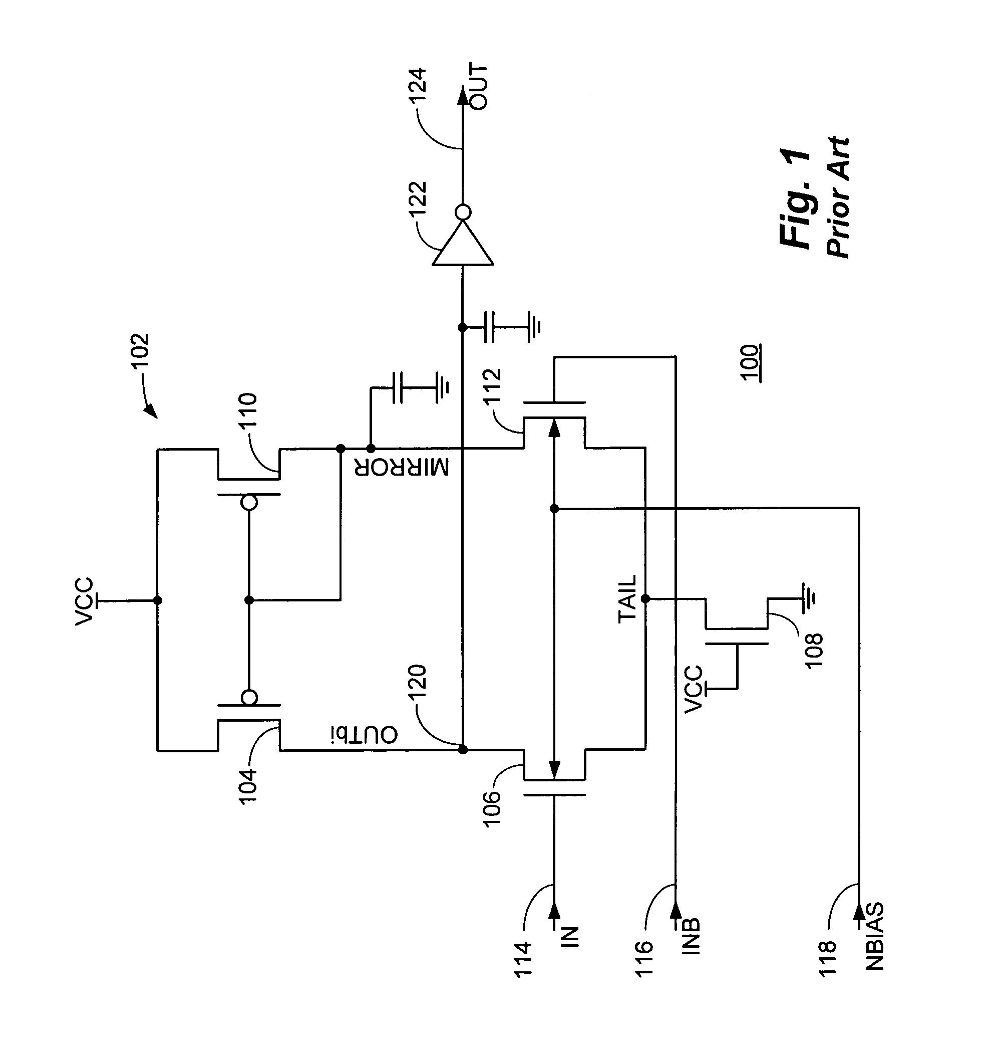
[0023] With reference now to FIG. 1, a schematic diagram of a conventional MOS differential amplifier 100 is shown. The conventional MOS differential amplifier 100 comprises, in pertinent part, a current mirror and differential pair circuit 102 comprising series connected P-channel transistor 104 and N-channel transistor 106 in parallel with series connected P-channel transistor 110 and N-channel transistor 112. The source terminals of transistors 104 and 110 are connected to a supply voltage source (VCC) while the source terminals of transistors 106 and 112 (node TAIL) are coupled to a reference voltage level of circuit ground through current source N-channel transistor 108 which has its gate terminal connected to VCC.

[0024] The gate terminals of transistors 104 and 110 are coupled together to the drain terminal of transistor 110 (node MIRROR) which has a parasitic capacitance as indicated. Transistors 104 and 100 thus form the well known current mirror circuit configuration. The ...


PUM


Abstract

A differential amplifier design and bias control technique of particular applicability for low voltage operation in which the threshold voltage of n-channel differential input transistors is controlled using substrate bias in order to allow a wider range of input signal levels. Further disclosed is a technique for controlling the substrate bias of the input transistors of a differential amplifier based on the level of the output of the amplifier in addition to a differential amplifier circuit capable of low voltage operation in which an additional bias current is introduced that enables the output pull-up current to be increased without increasing the pull-down current, as well as circuitry for optimizing the performance of the differential in both DDR-I and DDR-II operational modes.

Description

BACKGROUND OF THE INVENTION [0001] The present invention relates, in general, to the field of differential amplifiers. More particularly, the present invention relates to a differential amplifier circuit of especial applicability to low voltage operations and a bias technique for enabling the accommodation of an increased range of input levels. [0002] Differential amplifiers are utilized to amplify, and produce an output signal which is a function of the difference between two differential, or complementary, input signals and to thereby enable the detection of relatively weak signal levels while inherently rejecting noise common on the differential input lines. In this regard, conventional integrated circuit differential amplifier designs have included the provision of a differential pair of input transistors having a current mirror load and which are also coupled to a current source for providing a single output signal in response. However, as transistor dimensions and power supply...

Claims


Application Information

Patent Timeline
Patent Type & Authority Applications(United States)
IPC IPC(8): H03F1/30H03F3/45
CPCH03F3/45183H03F2200/513H03F2203/45684
Inventor HEIGHTLEY, JOHN D.FAUE, JON ALLAN
Owner PROMOS TECH INC
Why Eureka
Try Eureka