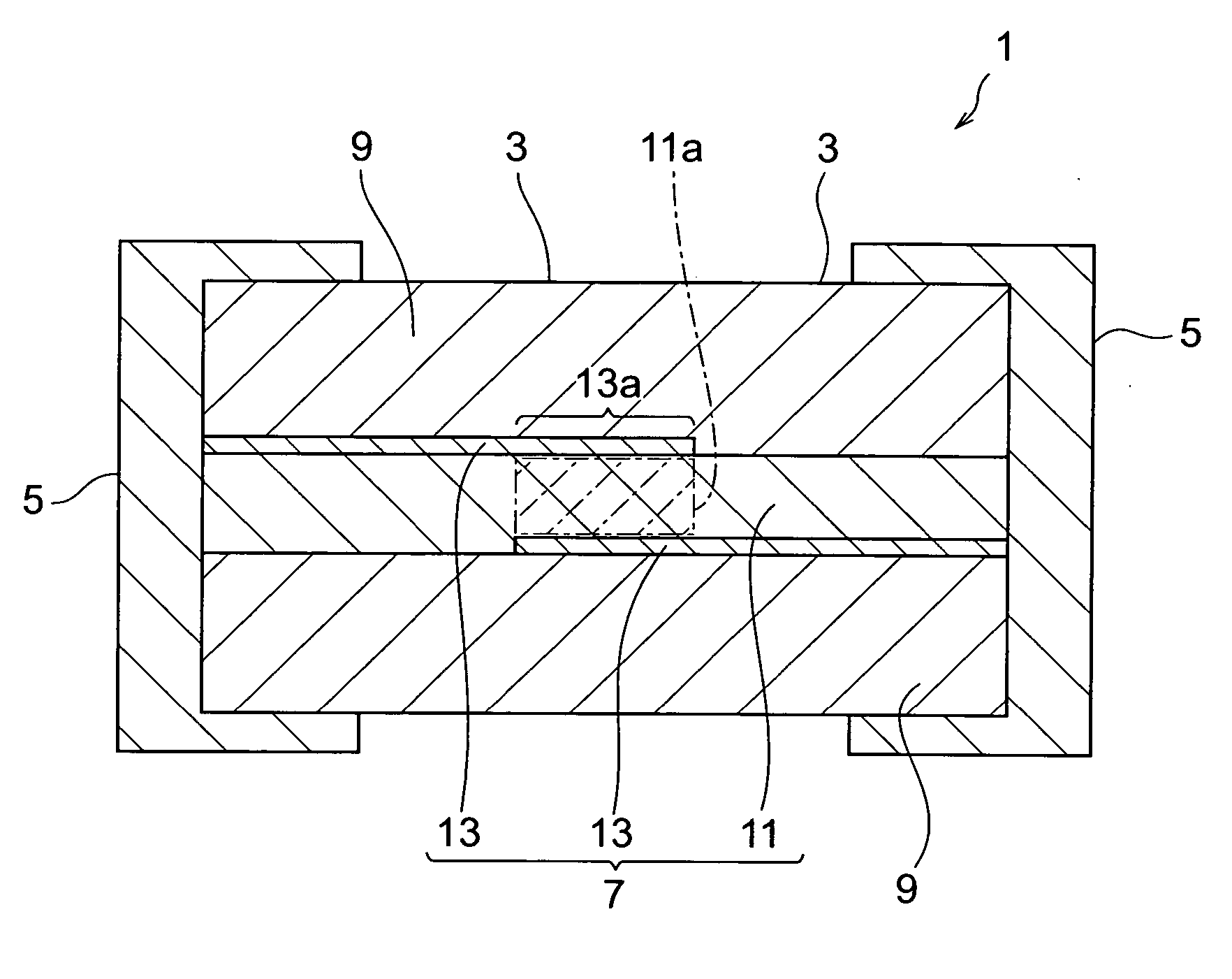
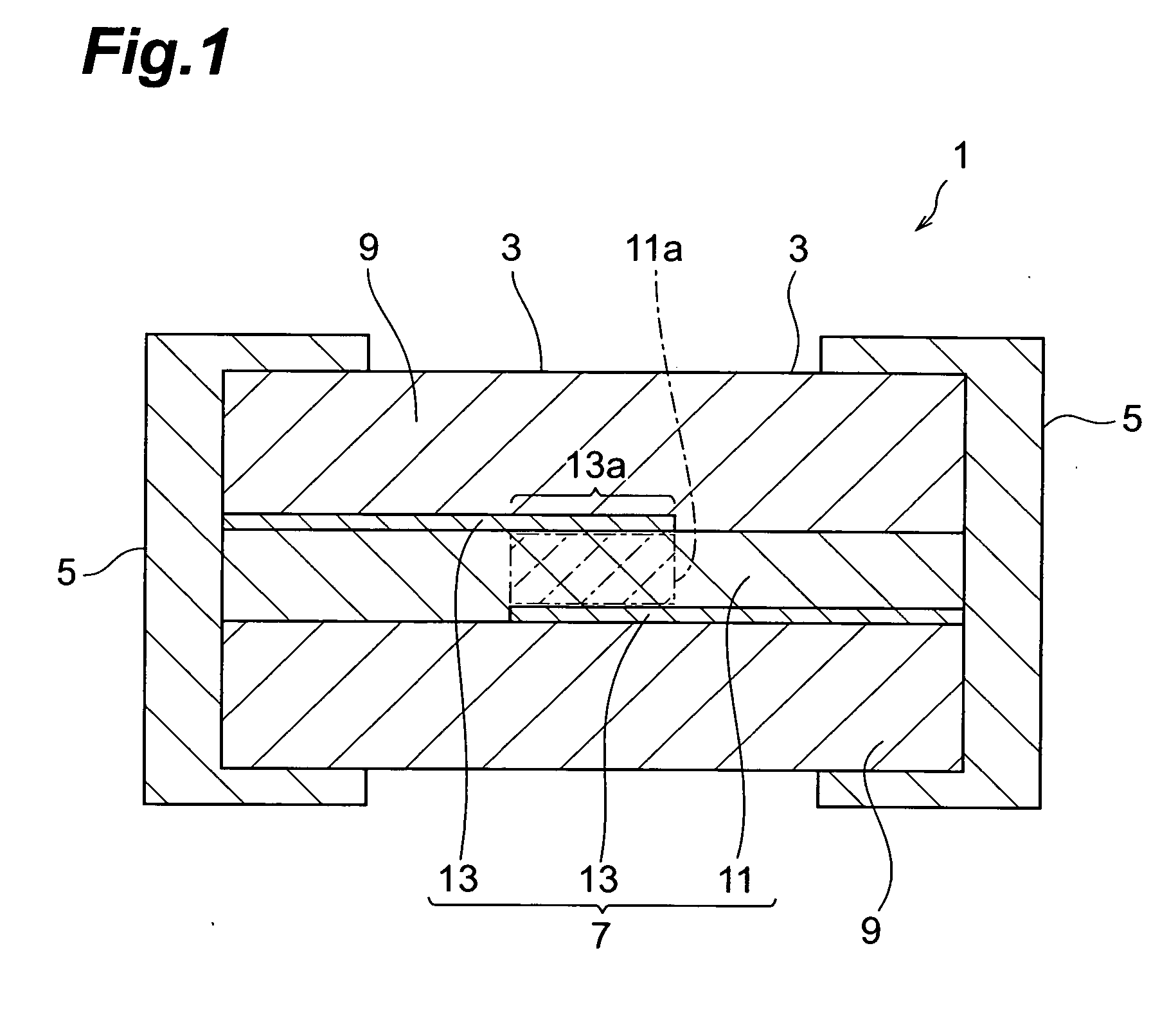
Multilayer chip varistor
a multi-layer chip and varistor technology, applied in the direction of fixed capacitor details, fixed capacitors, fixed capacitor terminals, etc., can solve the problems of reducing the resistance to esd, communication might be impossible, etc., and achieve good resistance and reduce the effect of electrostatic capacitan
- Summary
- Abstract
- Description
- Claims
- Application Information
AI Technical Summary
Benefits of technology
Problems solved by technology
Method used
Image

Examples
working example 1
[0068] A varistor material to be used for the varistor layer (first green sheet) was prepared by adding Pr (0.5 mol %), Co (1.5 mol %), Al (0.005 mol %), K (0.05 mol %), Cr (0.1 mol %), Ca (0.1 mol %), and Si (0.02 mol %) to ZnO (97.725%) with a purity of 99.9%. The varistor material to be used for the outer layer section (second green sheet) was prepared by adding Pr (0.5 mol %), Co (0.05 mol %), Al (0.005 mol %), K (0.05 mol %), Cr (0.1 mol %), Ca (0.1 mol %), and Si (0.02 mol %) to ZnO (99.175 mol %) with a purity of 99.9%. Also, electrically conductive paste for forming internal electrodes was prepared by mixing metal powder comprising Pd particles, organic binder, and organic solvent.
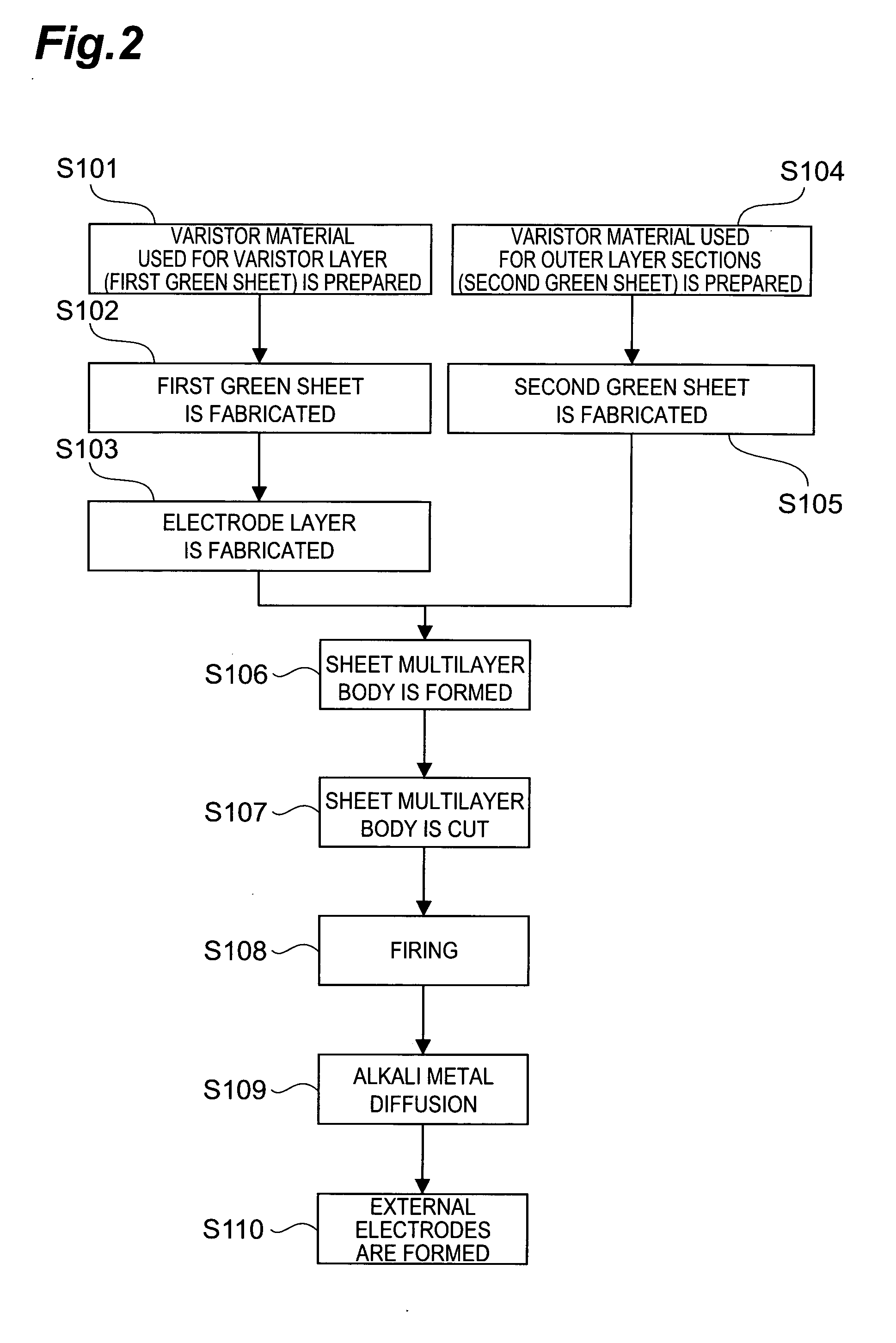
[0069] A multilayer chip varistor of a 1608 type was manufactured following the manufacturing process represented in FIG. 2 by using the above-described varistor material and electrically conductive paste. The surface area of the overlapping portions of the internal electrodes was set to 0.05 mm2....
working examples 2 and 3
[0071] Multilayer chip varistors of Working Examples 2 and 3 were obtained in the same manner as in Working Example 1, except that the amount of added Co in the varistor material used for the external outer sections (second green sheet) was set to 0.01 mol % and zero. Because the amount of added Co was changed with respect to that of Working Example 1, the amount of ZnO in Working Examples 2 and 3 was adjusted to obtain a total amount of ZnO and other metal atoms of 100 mol %.
working examples 4 to 7
[0072] Multilayer chip varistors of Working Examples 4 to 7 were obtained in the same manner as in Working Example 1, except that the amount of added Pr in the varistor material used for the external outer sections (second green sheet) was set to 0.05 mol %, 0.01 mol %, 0.005 mol %, and zero. Because the amount of added Pr was changed with respect to that of Working Example 1, the amount of ZnO in Working Examples 4 to 7 was adjusted to obtain a total amount of ZnO and other metal atoms of 100 mol %.
PUM
 Abstract
Description
Claims
Application Information
 - R&D
- Intellectual Property
- Life Sciences
- Materials
- Tech Scout
- Unparalleled Data Quality
- Higher Quality Content
- 60% Fewer Hallucinations
Browse by: Latest US Patents, China's latest patents, Technical Efficacy Thesaurus, Application Domain, Technology Topic, Popular Technical Reports.
© 2025 PatSnap. All rights reserved.Legal|Privacy policy|Modern Slavery Act Transparency Statement|Sitemap|About US| Contact US: help@patsnap.com