Method for treating a semiconductor surface to form a metal-containing layer

a metal-containing layer and semiconductor technology, applied in the field of semiconductor processing, can solve the problems of non-planar surface, degrade device performance, and challenge the scalability of thin gate dielectric films

Active Publication Date: 2005-12-15
NXP USA INC +1
View PDF7 Cites 72 Cited by
  • Summary
  • Abstract
  • Description
  • Claims
  • Application Information

AI Technical Summary

Problems solved by technology

However, if such thin films are formed using current ALD techniques, they are typically non-continuous until a substantial film thickness is reached, which requires a large number of ALD cycles.
This poses a challenge to the scalability of thin gate dielectric films.
Furthermore, due to the sparseness of nucleation sites, at time t4, voids 26 and 28 are still present, thus resulting in a non-planar surface which in turn may degrade device performance (e.g., higher leakage current).
Therefore, due to the sparseness of the nucleation sites, and the lack of reaction...

Method used


Image

  • Method for treating a semiconductor surface to form a metal-containing layer
  • Method for treating a semiconductor surface to form a metal-containing layer
  • Method for treating a semiconductor surface to form a metal-containing layer

Examples


Embodiment Construction

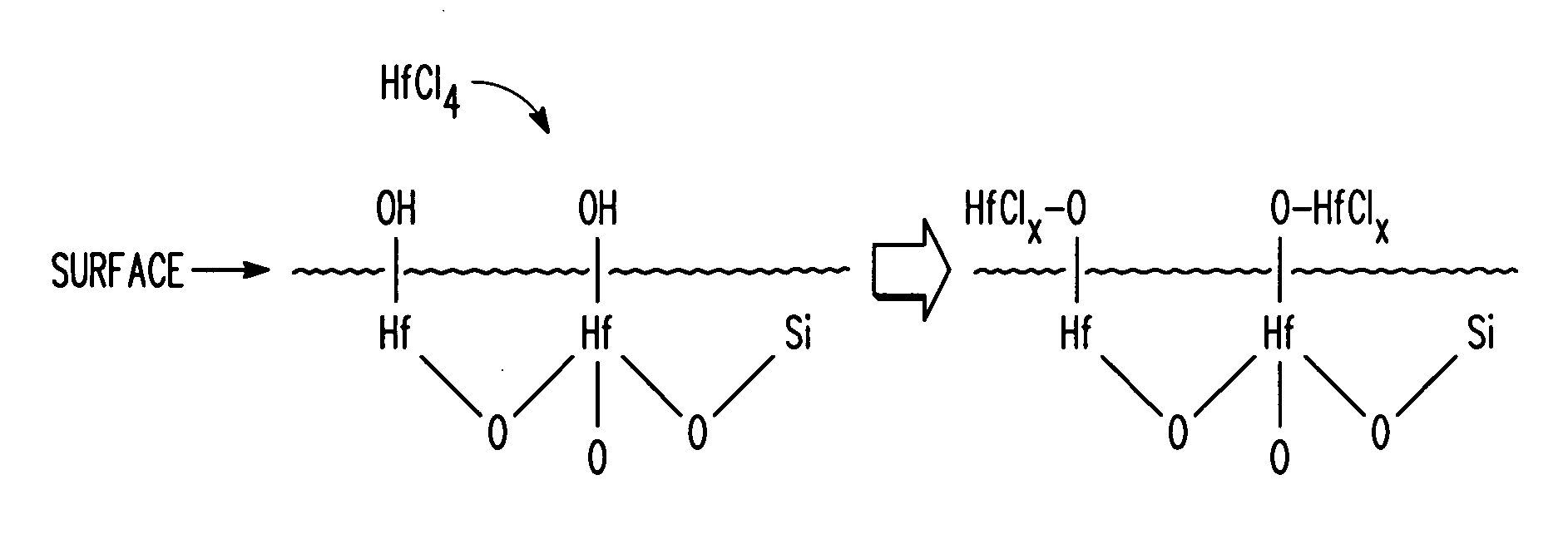
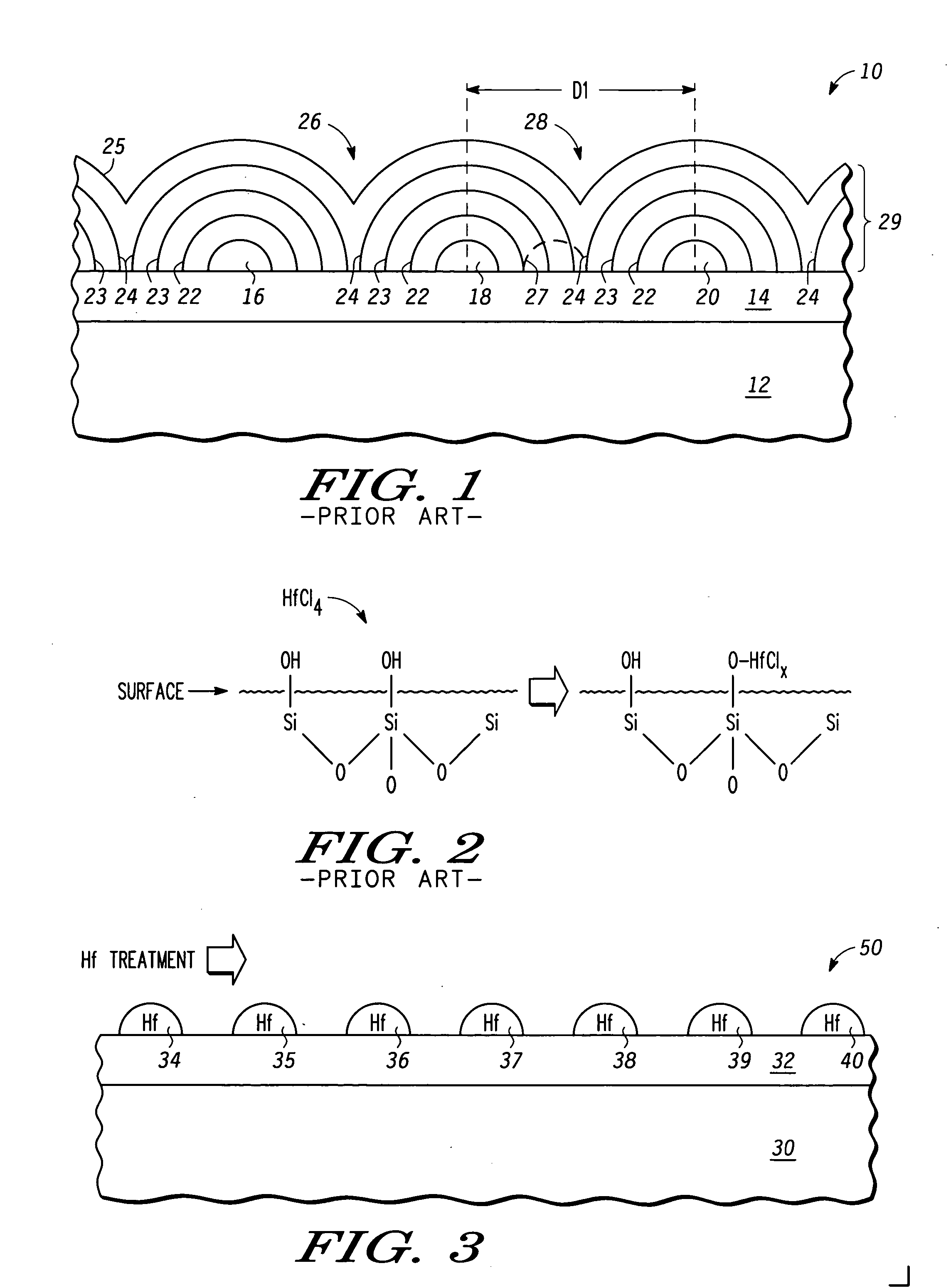
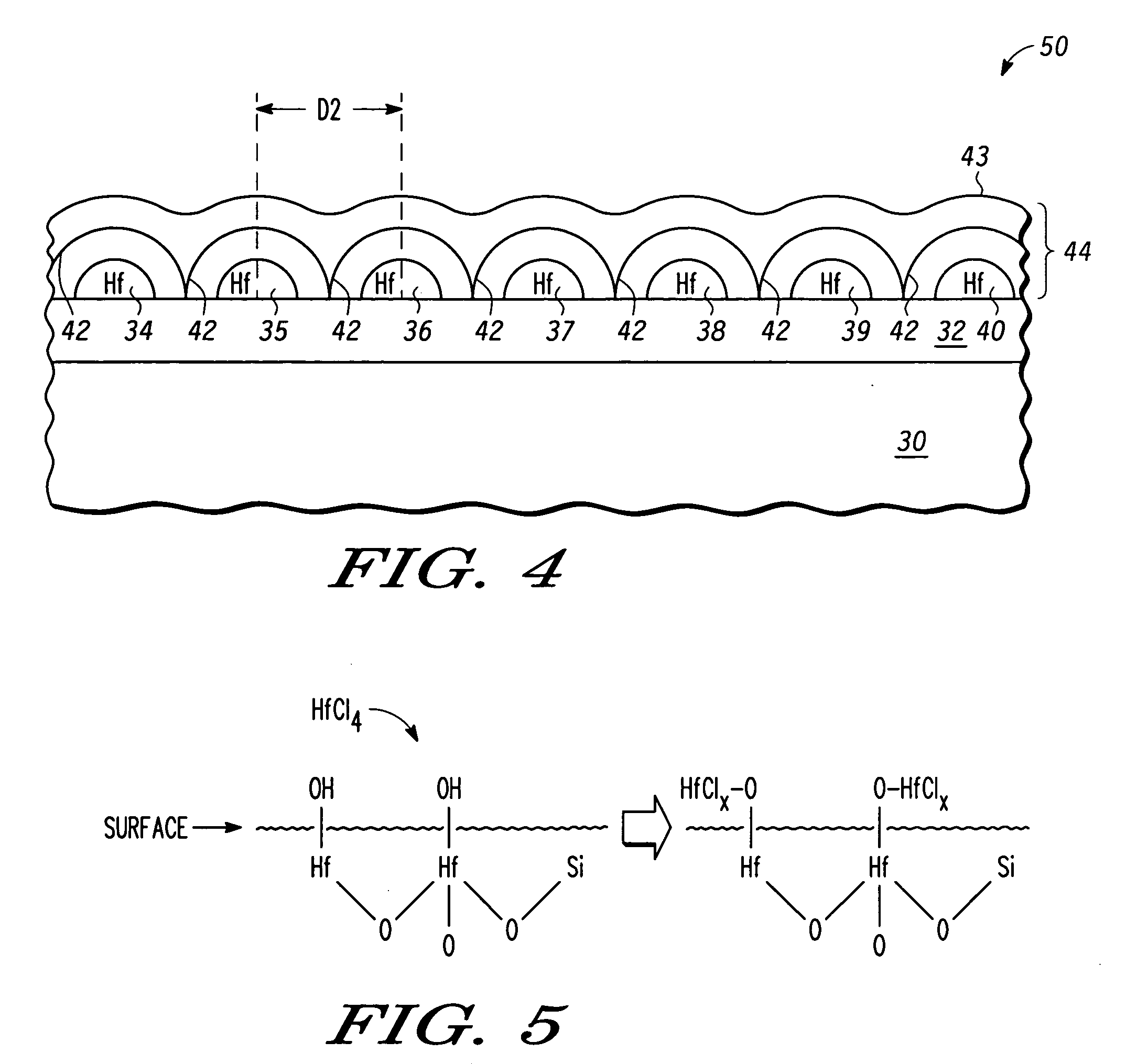
[0012] Through the use of a metal treatment of an exposed surface, the reactivity of nucleation sites may be increased for the subsequent ALD formation of a metal-containing layer. In one embodiment, the metal treatment is performed so that a uniformly spaced distribution of nucleation sites results where each nucleation site has increased reactivity. This may allow for a thinner continuous metal-containing layer in which a reduced number of voids is formed. This may therefore allow for the ability to increase scalability, improve electrical properties, and reduce leakage of thin high K gate dielectrics.

[0013] Illustrated in FIG. 3 is a semiconductor device 50 in which nucleation sites are formed. In FIG. 3, a semiconductor substrate 30 is provided. In one form substrate 30 is a bulk semiconductor such as silicon, silicon germanium, or germanium, but any of various semiconductor materials may be used to implement substrate 30. Alternatively, substrate 30 may be implemented as a sil...


PUM

PropertyMeasurementUnit
Thicknessaaaaaaaaaa
Densityaaaaaaaaaa
Semiconductor propertiesaaaaaaaaaa

Abstract

A method for treating a semiconductor surface to form a metal-containing layer includes providing a semiconductor substrate having an exposed surface. The exposed surface of the semiconductor substrate is treated by forming one or more metals overlying the semiconductor substrate but not completely covering the exposed surface of the semiconductor substrate. The one or more metals enhance nucleation for subsequent material growth. A metal-containing layer is formed on the exposed surface of the semiconductor substrate that has been treated. The treatment of the exposed surface of the semiconductor substrate assists the metal-containing layer to coalesce. In one embodiment, treatment of the exposed surface to enhance nucleation may be performed by spin-coating, atomic layer deposition (ALD), physical layer deposition (PVD), electroplating, or electroless plating. The one or more metals used to treat the exposed surface may include any rare earth or transition metal, such as, for example, hafnium, lanthanum, etc.

Description

FIELD OF THE INVENTION [0001] This invention relates generally to semiconductor processing, and more specifically, to methods for treating a surface to form a metal-containing layer. RELATED ART [0002] Future generation semiconductor devices will require thin gate dielectric films having a high dielectric constant (K). One technique known today for forming these thin gate dielectric films is atomic layer deposition (ALD). However, if such thin films are formed using current ALD techniques, they are typically non-continuous until a substantial film thickness is reached, which requires a large number of ALD cycles. This poses a challenge to the scalability of thin gate dielectric films. [0003] For example, FIG. 1 illustrates a semiconductor device 10 having a semiconductor substrate 12, an oxide layer 14 overlying semiconductor substrate 12, and a dielectric layer 29 overlying oxide layer 14. Semiconductor substrate 12 may be any kind of semiconductor substrate such as a silicon subst...

Claims


Application Information

Patent Timeline
IPC IPC(8): C23C16/02H01L21/314H01L21/316H01L21/44
CPCC23C16/0272H01L21/31645H01L21/3141H01L21/02181
Inventor SCHAEFFER, JAMES K.ROAN, DARRELLTRIYOSO, DINA H.ADETUTU, OLUBUNMI O.
Owner NXP USA INC
Why Eureka
Try Eureka