Method and apparatus for providing wafer-level capacitive decoupling

Inactive Publication Date: 2005-12-22
ALLLE INC
View PDF17 Cites 10 Cited by
  • Summary
  • Abstract
  • Description
  • Claims
  • Application Information

AI Technical Summary

Benefits of technology

[0012] One embodiment of the present invention provides capacitive decoupling on the surface of a semiconductor die, instead of providing the decoupling on a package or printed circuit board to which the semiconductor die is attached. In this embodiment, a surface of a semiconductor die includes exposed power and ground conductors, which are electricall

Problems solved by technology

As microprocessors become progressively faster, voltage noise in the microprocessor core is becoming a significant factor in limiting system performance.
This faster switching can result in significant “step currents,” which are caused for example by changing code patterns, sleep cycles, etc.
If this voltage drop (or any other form of voltage noise) causes the voltage at the microprocessor core to drop below a minimum voltage, Vmin, an error in the circuitry can potentially arise.
Hence, the voltage drop at the microprocessor core ca

Method used


Image

  • Method and apparatus for providing wafer-level capacitive decoupling
  • Method and apparatus for providing wafer-level capacitive decoupling
  • Method and apparatus for providing wafer-level capacitive decoupling

Examples


Embodiment Construction

[0027] The following description is presented to enable any person skilled in the art to make and use the invention, and is provided in the context of a particular application and its requirements. Various modifications to the disclosed embodiments will be readily apparent to those skilled in the art, and the general principles defined herein may be applied to other embodiments and applications without departing from the spirit and scope of the present invention. Thus, the present invention is not limited to the embodiments shown, but is to be accorded the widest scope consistent with the principles and features disclosed herein.

Voltage Noise

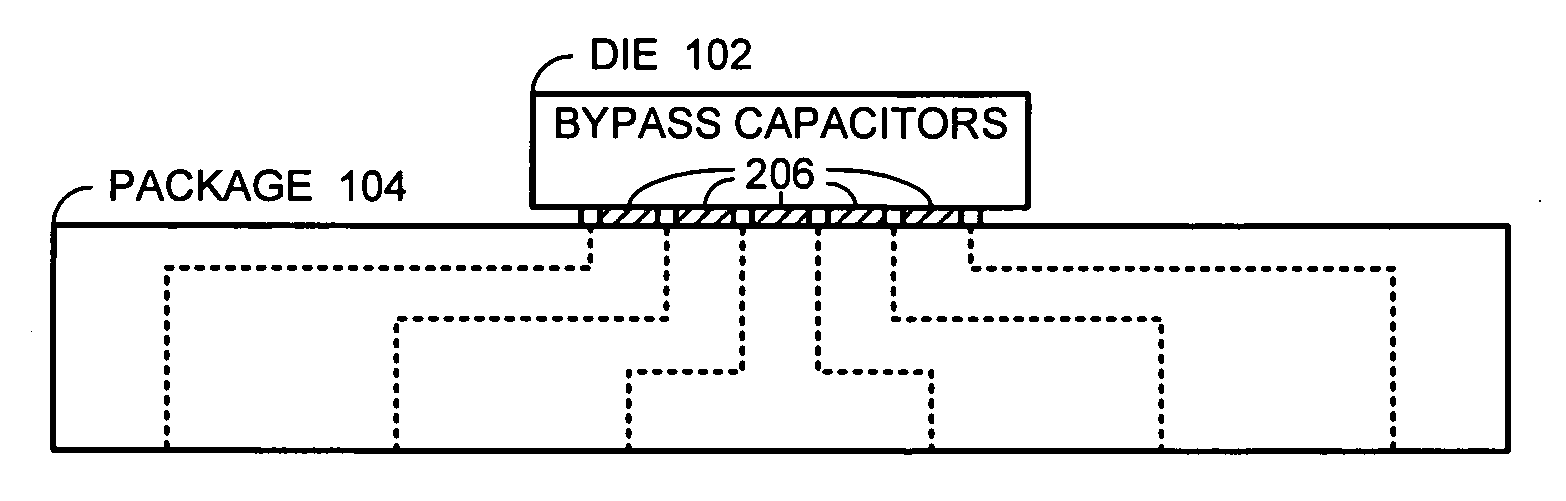
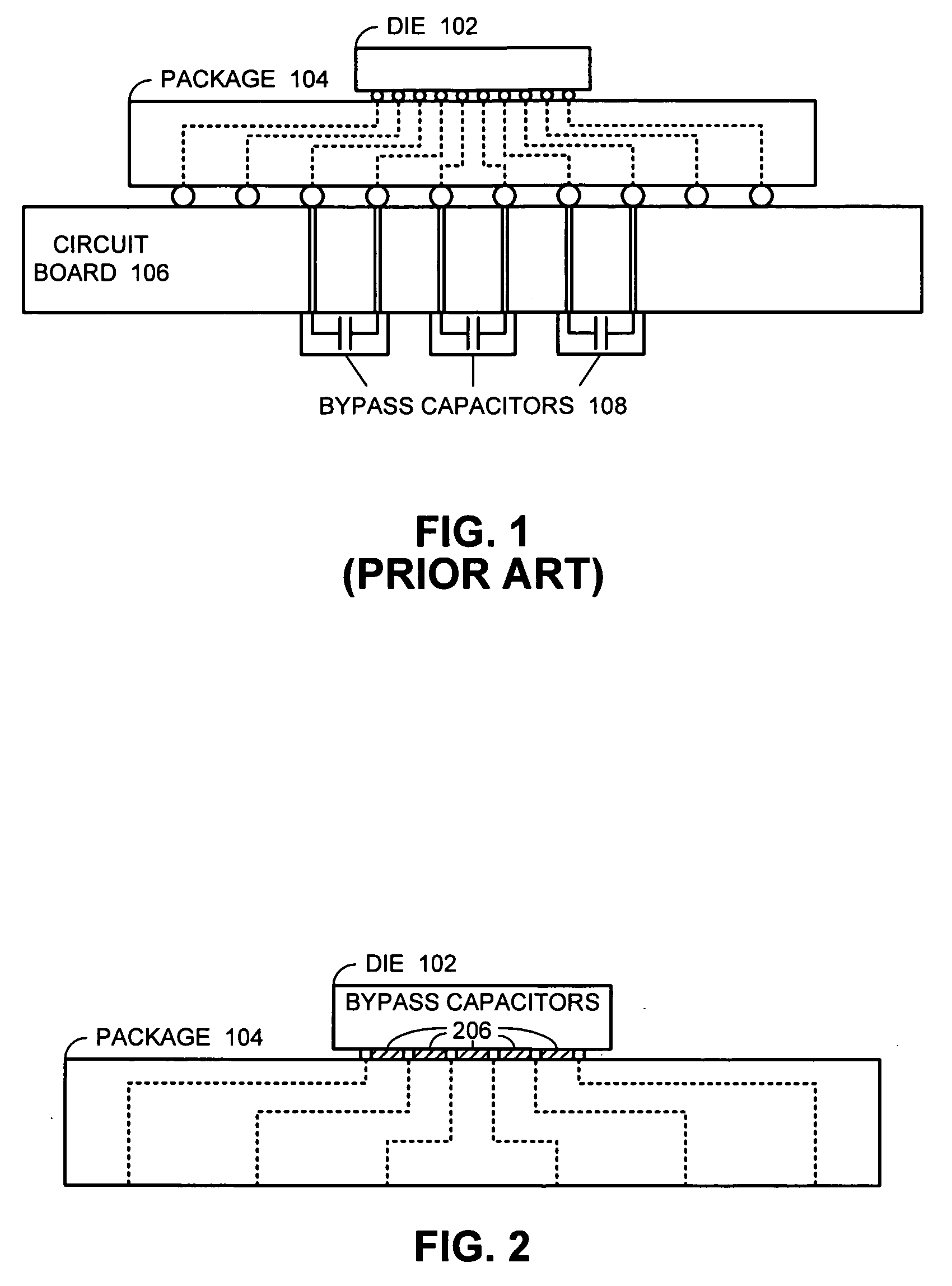
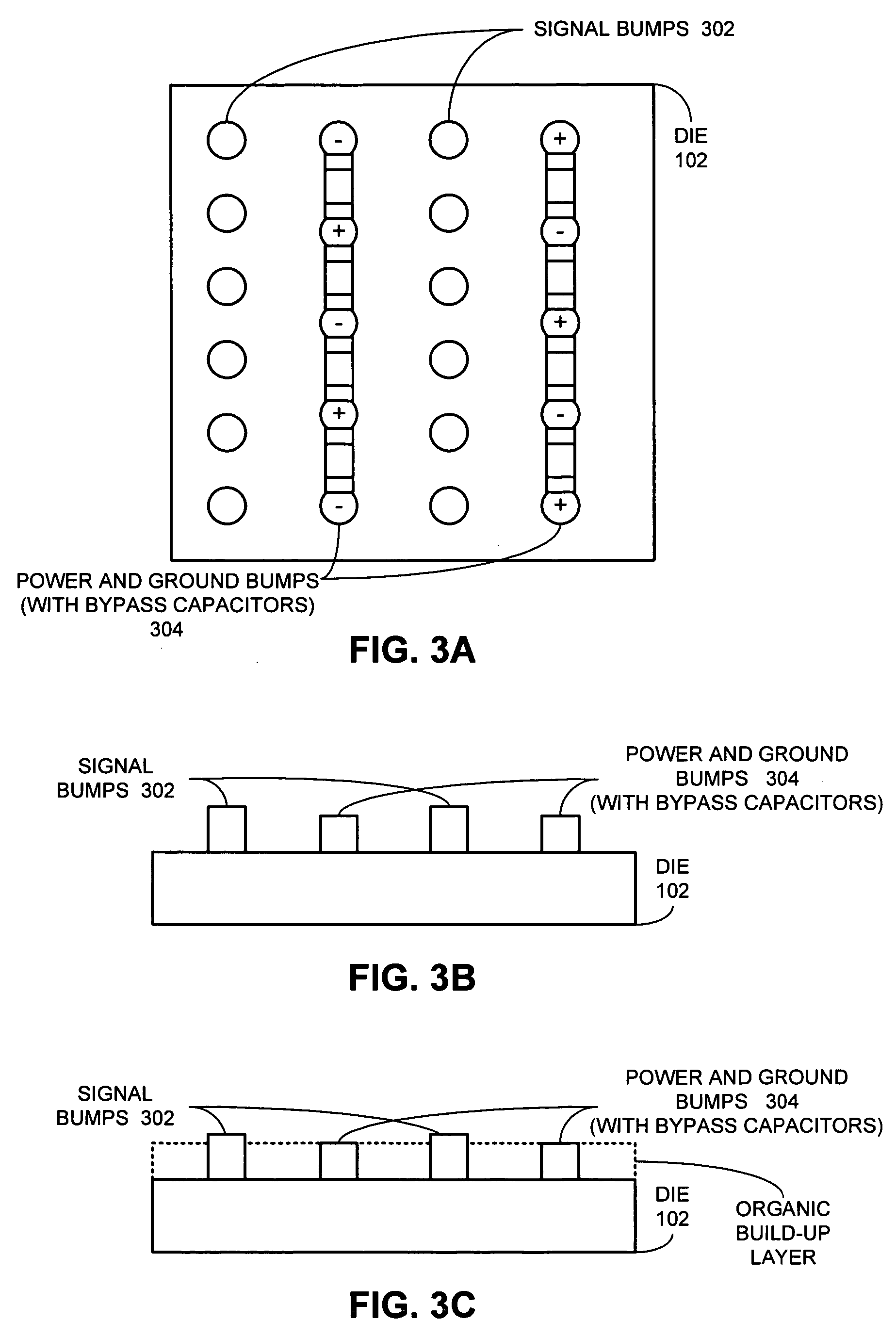
[0028] Voltage noise is typically caused by current steps. Current steps cause a voltage variation which is given by the product of the current step and the source impedance of a devices power system. In general terms,

Vnoise=L d[I(t)] / dt+I(t)R,

where L is the equivalent inductance the die sees from the power system, R is the DC resistance fr...


PUM


Abstract

One embodiment of the present invention provides capacitive decoupling on the surface of a semiconductor die, instead of providing the decoupling on a package or printed circuit board to which the semiconductor die is attached. In this embodiment, a surface of a semiconductor die includes exposed power and ground conductors, which are electrically coupled to internal power and ground nodes within the semiconductor die. To provide the wafer-level decoupling, a plurality of bypass capacitors are electrically coupled between pairs of exposed power and ground conductors, so that the plurality of bypass capacitors reduce voltage noise between the power and ground conductors on the semiconductor die.

Description

RELATED APPLICATION [0001] This application is a continuation-in-part of a pending U.S. patent application Ser. No. 10 / 871,845, filed Jun. 17, 2004 entitled, “Interposer Containing Bypass Capacitors for Reducing Voltage Noise in an IC Device,” by inventor William P. Cornelius. This application hereby claims priority under 35 U.S.C. §120 to the above-listed patent application. Moreover, the above-listed patent application is hereby incorporated by reference.BACKGROUND [0002] 1. Field of the Invention [0003] The present invention relates to techniques for reducing voltage noise in electrical circuits. More specifically, the present invention relates to a method and an apparatus for providing capacitive decoupling at the wafer level to reduce voltage noise on an integrated (IC) circuit device, such as a microprocessor chip. [0004] 2. Related Art [0005] As microprocessors become progressively faster, voltage noise in the microprocessor core is becoming a significant factor in limiting s...

Claims


Application Information

Patent Timeline
IPC IPC(8): H01L21/44H01L23/34H01L23/485H01L23/498H01L23/50H01L23/52
CPCH01L23/49822H01L2224/16235H01L24/73H01L2224/13099H01L2924/01015H01L2924/01027H01L2924/01029H01L2924/01082H01L2924/12044H01L2924/14H01L2924/15174H01L2924/15311H01L2924/15312H01L2924/19041H01L2924/19103H01L2924/19104H01L2924/19106H01L2924/30105H01L2924/30107H01L2924/3011H01L2924/01006H01L2924/01033H01L2924/014H01L2224/16225Y10S257/924H01L24/13H01L24/14H01L2224/1403H01L2224/14515H01L23/50
Inventor CORNELIUS, WILLIAM P.
Owner ALLLE INC
Why Eureka
Try Eureka