Method for manufacturing semiconductor substrate and semiconductor substrate

a manufacturing method and semiconductor technology, applied in the direction of semiconductor devices, electrical devices, chemistry apparatus and processes, etc., can solve the problems of substantially impossible to remove hydrogen from the soi substrate on which the semiconductor elements have been formed, the threshold voltage shift is caused on the semiconductor elements, and the impurity properties of the semiconductor elements change, so as to achieve the effect of reducing adverse effects

Inactive Publication Date: 2005-12-22
SHARP KK
View PDF6 Cites 210 Cited by
  • Summary
  • Abstract
  • Description
  • Claims
  • Application Information

AI Technical Summary

Benefits of technology

[0012] Under these circumstances, the present invention has been achieved. As to a semiconductor substrate obtained by a technique of forming a peel layer in the substrate and then peeling part of the substrate off along the peel layer, an object of the present invention is to eliminate adverse effects caused by the diffusion of a substance for peeling the substrate into semiconductor elements which will be or have been formed on the semiconductor substrate.
[0065] If the step of peeling part of the semiconductor substrate by heat treatment is carried out after the diffusion inhibiting substance is thus introduced into the semiconductor substrate, the diffusion inhibiting substance inhibits migration of the peeling substance which is likely to be diffused during the heat treatment.
[0066] That is, the peeling substance becomes less likely to migrate to part of the semiconductor substrate in which a semiconductor layer will be formed in a later step or to the semiconductor layer which has already been formed in the semiconductor substrate. As a result, the peeling substance becomes less possible to cause adverse effects on threshold value control.
[0067] After the peeling step, the anti-diffusion layer and the peel layer are preferably removed together. This prevents adverse effects on threshold value control by the peeling substance in the peel layer or the diffusion inhibiting substance in the anti-diffusion layer.

Problems solved by technology

As a result, adverse effects such as a shift in threshold voltage are caused on the semiconductor elements.
Such high temperature environment may change the impurity properties of the semiconductor elements.
Therefore, it is substantially impossible to remove hydrogen from the SOI substrate on which the semiconductor elements have been formed.
Further, since the second substrate is subjected to a temperature as high as 800° C. or more, the choice of material for the second substrate is limited.

Method used


Image

  • Method for manufacturing semiconductor substrate and semiconductor substrate
  • Method for manufacturing semiconductor substrate and semiconductor substrate
  • Method for manufacturing semiconductor substrate and semiconductor substrate

Examples


embodiment 1

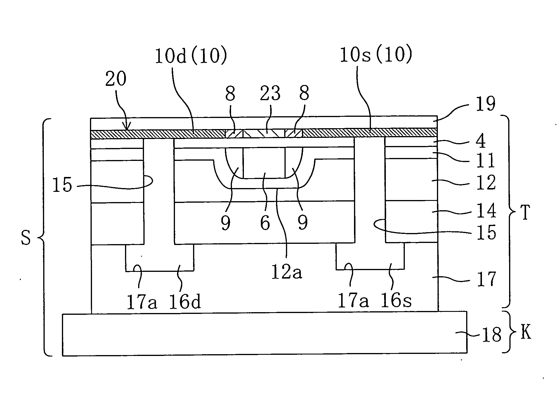
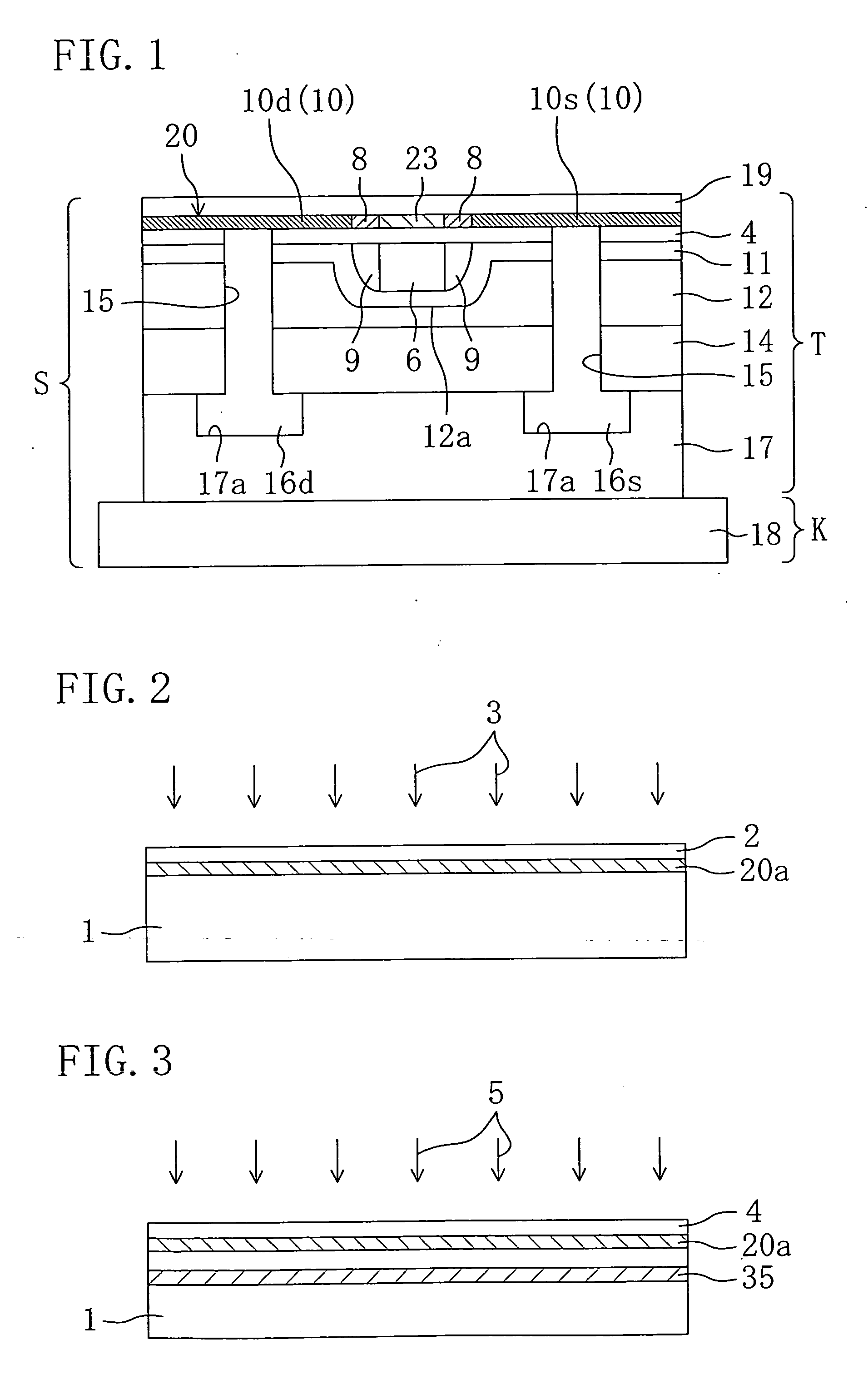
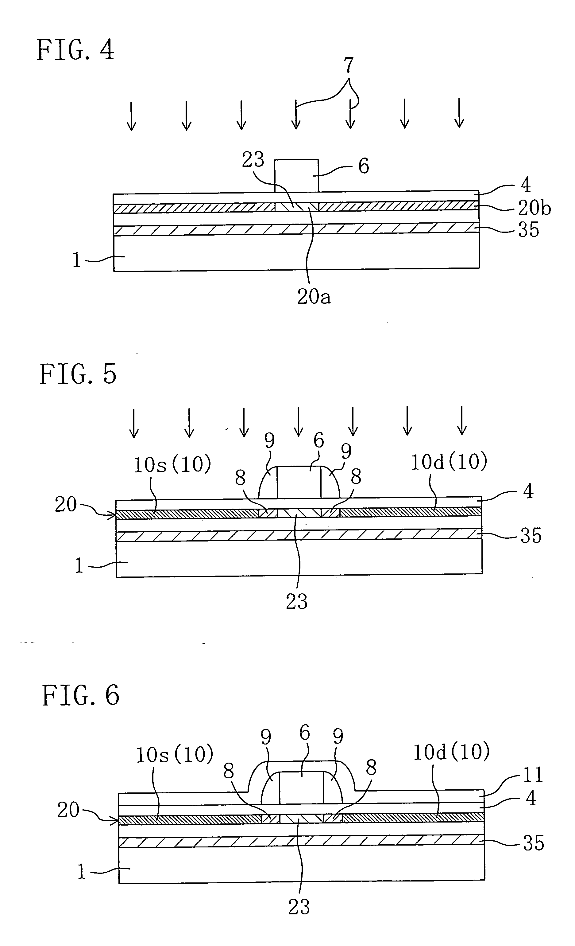
[0108] FIGS. 1 to 11 are sectional views according to Embodiment 1 of the present invention. In Embodiment 1, a semiconductor element T is completed on a substrate and then the substrate is bonded to another substrate K (hereinafter referred to as substrate K) to obtain a semiconductor device S. For the sake of convenience, expressions related to position and direction such as top and bottom, right and left, are based on the drawings when viewed from the front.

[0109] In general, the semiconductor element T includes a plurality of NMOS transistors and / or PMOS transistors formed on a single substrate. However, for a simple explanation, it is assumed hereinafter that a single NMOS transistor is formed on the substrate. Though not clearly mentioned, the PMOS transistor can be formed in a like manner by optionally changing the conductivity of ions to be implanted. It should be understood that there is no intention of excluding the case of forming a single transistor. Although no referen...

embodiment 2

[0154] FIGS. 13 to 23 are sectional views illustrating a semiconductor substrate and a method for manufacturing the same according to Embodiment 2 of the present invention. In the following embodiments, the same components as those shown in FIGS. 1 to 11 are given with the same reference numerals and a detailed explanation is omitted.

[0155] In this embodiment, a silicon substrate layer L in which a semiconductor layer 20 will be formed is transferred to a substrate K in advance and then the semiconductor element T is formed thereon.

[0156] In general, the semiconductor element T includes a plurality of NMOS transistors and / or PMOS transistors formed on a single substrate. However, for a simple explanation, it is assumed that a single NMOS transistor is formed on the substrate. Though not clearly mentioned, the PMOS transistor can be formed in a like manner by optionally changing the conductivity of ions to be implanted. It should be understood that there is no intention of excludin...

embodiment 3

[0184] FIGS. 24 to 32 are sectional views illustrating a semiconductor substrate and a method for manufacturing the same according to Embodiment 3 of the present invention.

[0185] In this embodiment, part of the semiconductor element T is formed before the bonding step and the other part of the semiconductor element T is formed after the bonding step.

[0186]FIG. 24 is a sectional view schematically illustrating a semiconductor device S including a substrate K and a semiconductor element T. In general, the semiconductor element T includes a plurality of NMOS transistors and / or PMOS transistors formed on a single substrate. However, for a simple explanation, it is assumed hereinafter that a single NMOS transistor is formed on the substrate. Though not clearly mentioned, the PMOS transistor can be formed in a like manner by optionally changing the conductivity of ions to be implanted. It should be understood that there is no intention of excluding the case of forming a single transisto...


PUM

PropertyMeasurementUnit
temperatureaaaaaaaaaa
softening pointaaaaaaaaaa

Abstract

A method for manufacturing a semiconductor substrate comprises the steps of: forming a gate oxide film as an insulating layer on the surface of a semiconductor substrate; implanting boron ions for inhibiting the migration of a peeling substance in the semiconductor substrate to form an anti-diffusion layer in the semiconductor substrate; activating boron in the anti-diffusion layer by heat treatment; implanting hydrogen ions into the semiconductor substrate to form a peel layer in part of the semiconductor substrate at a side of the anti-diffusion layer opposite to the gate oxide film; bonding a glass substrate to the surface of the semiconductor substrate where the gate oxide film has been formed; and heat-treating the semiconductor substrate to separate part of the semiconductor substrate along the peel layer.

Description

CROSS-REFERENCE TO RELATED APPLICATION [0001] This non-provisional application claims priority under 35 U.S.C. §119(a) on Patent Application No. 2004-181527 filed in Japan on Jun. 18, 2004, the entire contents of which are hereby incorporated by reference.BACKGROUND OF THE INVENTION [0002] (a) Field of the Invention [0003] The present invention relates to a method for manufacturing a semiconductor substrate and a semiconductor substrate. [0004] (b) Description of Related Art [0005] So far, there have been known SOI (silicon-on-insulator) substrates including an insulating layer and a monocrystalline silicon layer formed on the insulating layer. If elements such as transistors are formed on the SOI substrate, parasitic capacitance decreases and insulation resistance increases. That is, the SOI substrate allows an increase in packing density and an improvement in performance of the elements. The insulating layer is, for example, a silicon oxide (SiO2) film. [0006] Aiming at an increas...

Claims


Application Information

Patent Timeline
Patent Type & Authority Applications(United States)
IPC IPC(8): B32B9/04H01L21/68
CPCH01L21/6835H01L24/97H01L2924/1305H01L2924/1301H01L2924/13091H01L2924/01033H01L2924/01019H01L2221/68363H01L2924/01002H01L2924/01005H01L2924/0101H01L2924/01013H01L2924/01015H01L2924/01018H01L2924/01054H01L2924/01057H01L2924/01073H01L2924/01074H01L2924/04953H01L2924/30105H01L2924/01006H01L2924/00H01L2924/12042H01L27/12H01L21/18
Inventor FUKUSHIMA, YASUMORITAKAFUJI, YUTAKA
Owner SHARP KK
Why Eureka
Try Eureka