High-reliability solder joint for printed circuit board and semiconductor package module using the same

Inactive Publication Date: 2005-12-22
SAMSUNG ELECTRONICS CO LTD
View PDF9 Cites 19 Cited by
  • Summary
  • Abstract
  • Description
  • Claims
  • Application Information

AI Technical Summary

Benefits of technology

[0021] According to the invention, the printed circuit board has the buffer layer adjacent the first terminal connected with the solder ball, and the semiconductor package has the three-dimensional pillar-shaped UBM formed on the input/output pad connected with the sold

Problems solved by technology

Consequently, and because of solder joint reliability (SJR) problems, the performan

Method used


Image

  • High-reliability solder joint for printed circuit board and semiconductor package module using the same
  • High-reliability solder joint for printed circuit board and semiconductor package module using the same
  • High-reliability solder joint for printed circuit board and semiconductor package module using the same

Examples


Embodiment Construction

[0031] The invention will now be described more fully with reference to the accompanying drawings, in which exemplary embodiments of the invention are shown. The invention may, however, be embodied in many different forms and should not be construed as being limited to the embodiments set forth herein; rather, these embodiments are provided so that this disclosure will be thorough and complete and will fully convey the concept of the invention to those skilled in the art.

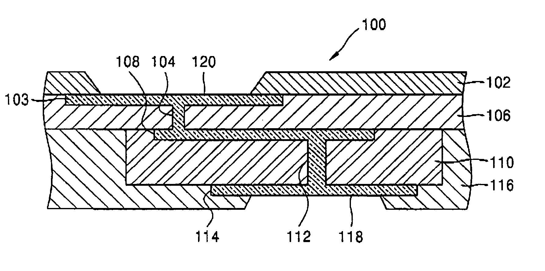
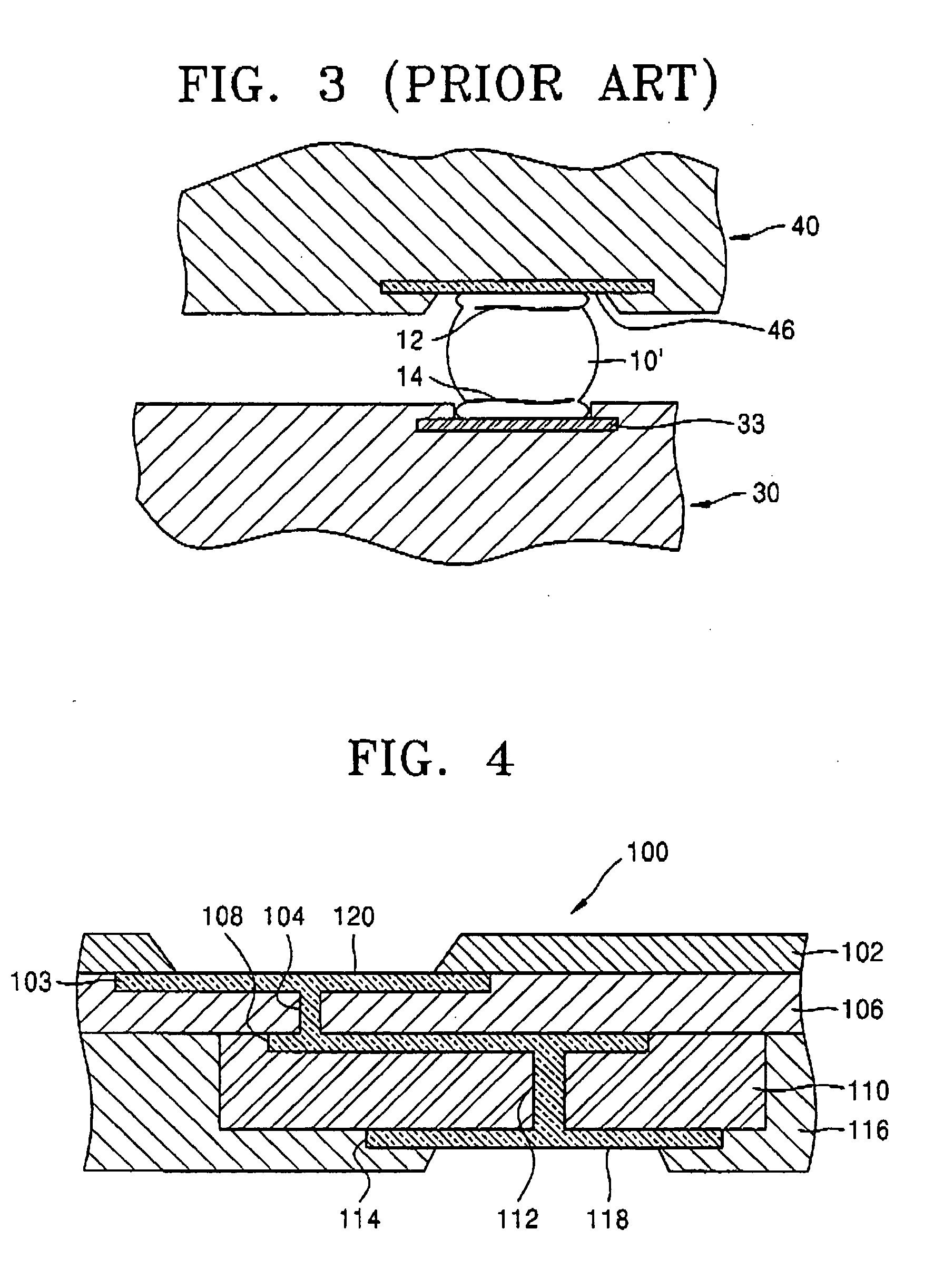
[0032]FIG. 4 is a sectional view illustrating a printed circuit board for improving solder joint reliability (SJR) according to one embodiment of the invention.

[0033] A printed circuit board 100 to improve the SJR is a multi-layered printed circuit board where insulating layers 102, 106 and 116 and print circuit patterns 103, 108 and 114 are alternately layered. The printed circuit board 100 has a first terminal 118 exposed externally of the printed circuit board in a printed circuit pattern to be connected with a...


PUM


Abstract

A printed circuit board and a semiconductor package module using the same in which solder joint reliability (SJR) is improved. The printed circuit board includes: a first terminal exposed to the external of the printed circuit board in a print circuit pattern to be connected to a solder ball of a semiconductor package; a second terminal exposed to the external of the printed circuit board in the printed circuit pattern to be connected to another printed circuit board; and a buffer layer, which is an insulating layer formed adjacent the first terminal, being formed of a thermal absorption material, e.g. an elastomer, configured to absorb thermal stress caused by any difference of coefficients of thermal expansion between the semiconductor package and the first terminal, wherein the printed circuit board is a multi-layered printed circuit board including alternately layered insulators and printed circuit patterns.

Description

BACKGROUND OF THE INVENTION [0001] This application claims the priority of Korean Patent Application No. 2004-41854, filed on Jun. 8, 2004, in the Korean Intellectual Property Office, the disclosure of which is incorporated herein in its entirety by reference. 1. FIELD OF THE INVENTION [0002] This disclosure invention relates to a printed circuit board and a semiconductor package module using the same, and more particularly to stress problems caused by a difference in coefficients of thermal expansion between the semiconductor package and the printed circuit board. 2. DESCRIPTION OF THE RELATED ART [0003] A wafer level package (WLP) in which a semiconductor package is assembled at a wafer level represents an important recent advance over plastic packages that use a conventional wire bonding process. In recent years, wafer level package applications include the mounting of plural wafer level packages-whether of the same circuit type or different circuit types-on a single printed circ...

Claims


Application Information

Patent Timeline
IPC IPC(8): H01L23/12H01L21/288H01L21/44H01L21/60H01L23/32H01L23/373H01L23/485H01L23/498H01L23/50H05K1/02H05K1/11H05K3/28H05K3/34
CPCH01L21/2885H01L2924/014H01L23/49816H01L24/11H01L24/16H01L2224/13099H01L2924/01013H01L2924/01022H01L2924/01029H01L2924/01047H01L2924/01078H01L2924/01079H01L2924/01082H05K1/0271H05K1/113H05K3/28H05K3/3436H05K2201/0133H05K2201/0187H05K2201/0373H05K2201/09436H01L2924/01006H01L2924/01024H01L2924/01033H01L23/3735H01L2224/05001H01L2224/05022H01L2224/05024H01L2224/05026H01L2224/05085H01L2224/05124H01L2224/05147H01L2224/05155H01L2224/05166H01L2224/05171H01L2224/05548H01L2224/05639H01L2224/05644H01L2224/05647H01L2224/05655H01L2224/16237H01L2924/351Y02P70/50H01L2924/00H01L2924/00014H01L23/12H01L23/50
Inventor JEONG, SE-YOUNGOH, SE-YONG
Owner SAMSUNG ELECTRONICS CO LTD
Why Eureka
Try Eureka