Method of manufacturing semiconductor device

a manufacturing method and semiconductor technology, applied in the direction of semiconductor devices, basic electric elements, electrical appliances, etc., can solve the problems of difficult to obtain a high frequency over 100 ghz, limit to and difficult to manufacture a gate electrode having a gate length of about 0.1 m long, etc., to achieve the effect of simple method and shorten the gate length

Inactive Publication Date: 2005-12-22
MITSUBISHI ELECTRIC CORP
View PDF2 Cites 3 Cited by
  • Summary
  • Abstract
  • Description
  • Claims
  • Application Information

AI Technical Summary

Benefits of technology

[0010] According to the invention, it is possible to shorten a gate length by diagonally tilting a gate electrode by a simple method. Further, along with the foregoing, a cutoff frequency can be raised, and a high-frequency semiconductor can be realized.

Problems solved by technology

However, in the current EB (electron beam) exposure technique, there is a limit to shorten a gate length, and it is difficult to manufacture a gate electrode having a gate length being about 0.1 μm long.
Therefore, in the conventional MESFET (Metal Semiconductor Field Effect Transistor) and HEMT (High Electron Mobility Transistor), it has been difficult to obtain a high frequency over 100 GHz.
However, in the conventional methods of manufacturing a semiconductor device, there is a problem that a step of manufacturing a semiconductor device becomes complicated since a gate electrode is diagonally formed.

Method used


Image

  • Method of manufacturing semiconductor device
  • Method of manufacturing semiconductor device
  • Method of manufacturing semiconductor device

Examples


first embodiment

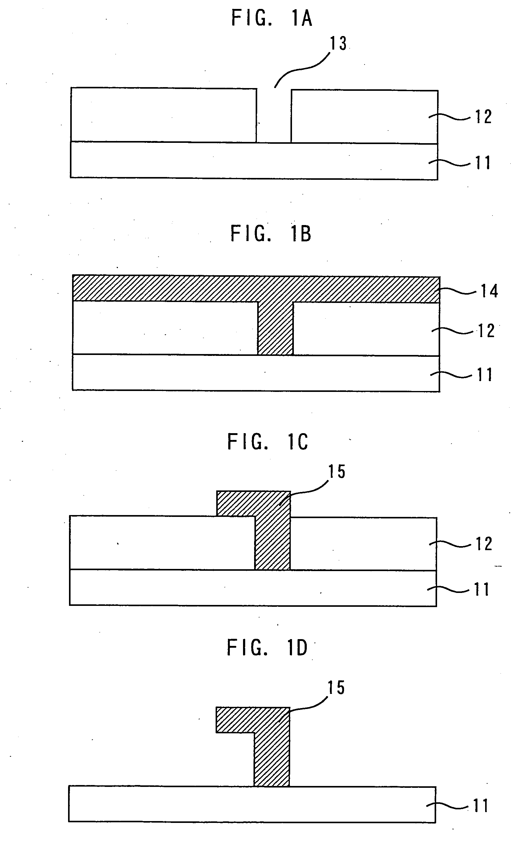
[0023] Descriptions will be hereinafter given of a method of manufacturing a semiconductor device according to a first embodiment of the invention with reference to FIGS. 1A-1D, 2A, 2B, 3 and 4.

[0024] First, as shown in FIG. 1A, an insulating film 12 made of SiN or the like is formed on a semiconductor substrate 11 made of GaAs or the like. Then, an opening 13 is formed in the insulating film 12 by EB or photolithography.

[0025] Next, as shown in FIG. 1B, a metal film 14 made of Al or the like is formed on a whole area to infill the opening 13. Then, as shown inFIG. 1C, the metal film 14 is provided with patterning by photo lithography to form a gate electrode 15 having a Γ-shape cross section. After that, as shown in FIG. 1D, the insulating film 12 is removed. By the foregoing steps, the gate electrode is formed on the semiconductor substrate.

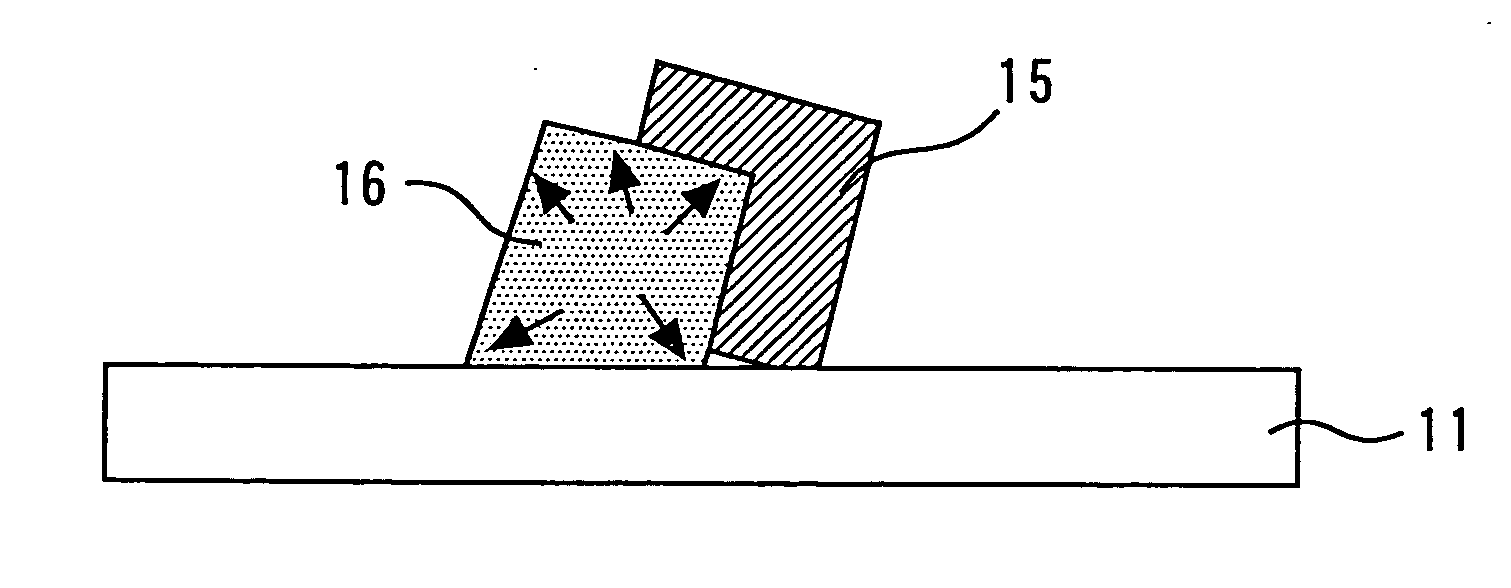
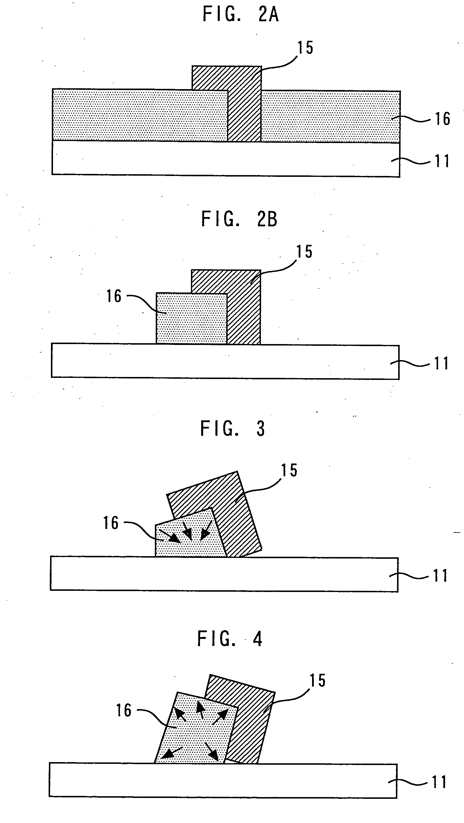
[0026] Next, as shown in FIG. 2A, a resist 16 is formed on a whole area of the semiconductor substrate 11. Then, as shown in FIG. 2B, by ex...

second embodiment

[0030] In the first embodiment, the cross section shape of the gate electrode is Γ. Meanwhile, in a second embodiment, a gate electrode 17 having a T-shape cross section as shown in FIG. 5 is used, or a gate electrode 18 having a Y-shape cross section as shown in FIG. 6 is used. In the case that a cross section of the gate electrode is T shape or Y shape as above, the resist gets in below the gate electrode, and shrinkage or expansion force is easily applied similarly to in the case of Γ shape in the first embodiment. Therefore, in the second embodiment, effects similar to in the first embodiment can be obtained.

third embodiment

[0031] In the third embodiment, a drain electrode 19 and a source electrode 20 are provided on the semiconductor substrate 11, and the gate electrode 15 is tilted to the source side. Thereby, without shifting an exposure position of the gate electrode 15 to the source side, a distance between the drain electrode 19 and the gate electrode 15 can be lengthened. Therefore, it is possible to reduce a capacity Cgd between the gate and the drain, and increase a withstand pressure Vgdo between the gate and the drain. Thereby, not only a high-frequency semiconductor device can be realized, but also a high-gain and high-withstanding pressure semiconductor device can be realized.


PUM

PropertyMeasurementUnit
gate lengthaaaaaaaaaa
frequencyaaaaaaaaaa
volumeaaaaaaaaaa

Abstract

A method of manufacturing a semiconductor device includes forming a gate electrode on a semiconductor substrate, forming a resist on the semiconductor substrate so that the resist contacts only one side face of the gate electrode, and tilting the gate electrode by shrinking or expanding the resist.

Description

BACKGROUND OF THE INVENTION [0001] 1. Field of the Invention [0002] The present invention relates to a method of manufacturing a semiconductor device capable of realizing a high-frequency semiconductor. [0003] 2. Background Art [0004] In order to realize a high-frequency semiconductor device, it is the most effective means that a gate length is shortened and a cutoff frequency is raised. However, in the current EB (electron beam) exposure technique, there is a limit to shorten a gate length, and it is difficult to manufacture a gate electrode having a gate length being about 0.1 μm long. [0005] Therefore, in the conventional MESFET (Metal Semiconductor Field Effect Transistor) and HEMT (High Electron Mobility Transistor), it has been difficult to obtain a high frequency over 100 GHz. [0006] Meanwhile, a method, wherein a gate length is shortened by diagonally forming a gate electrode is suggested (for example, refer to Japanese Unexamined Patent Application Publication No. H05-12934...

Claims


Application Information

Patent Timeline
Patent Type & Authority Applications(United States)
IPC IPC(8): H01L21/285H01L21/338H01L29/423H01L29/812
CPCH01L21/28593H01L29/42316H01L29/8124
Inventor HASUIKE, ATSUSHI
Owner MITSUBISHI ELECTRIC CORP
Why Eureka
Try Eureka