

Semiconductor device and method for manufacturing the same
a technology of semiconductors and semiconductors, applied in the direction of semiconductor devices, electrical equipment, transistors, etc., can solve the problems of chip area reduction, achieve the effect of reducing the gate length of the second mis transistor, reducing the amount of current, and minimizing the chip area
- Summary
- Abstract
- Description
- Claims
- Application Information
AI Technical Summary
Benefits of technology
Problems solved by technology
Method used
Image

Examples
embodiment 1
[0043] A semiconductor device manufacturing method according to Embodiment 1 of the present invention will be described below.
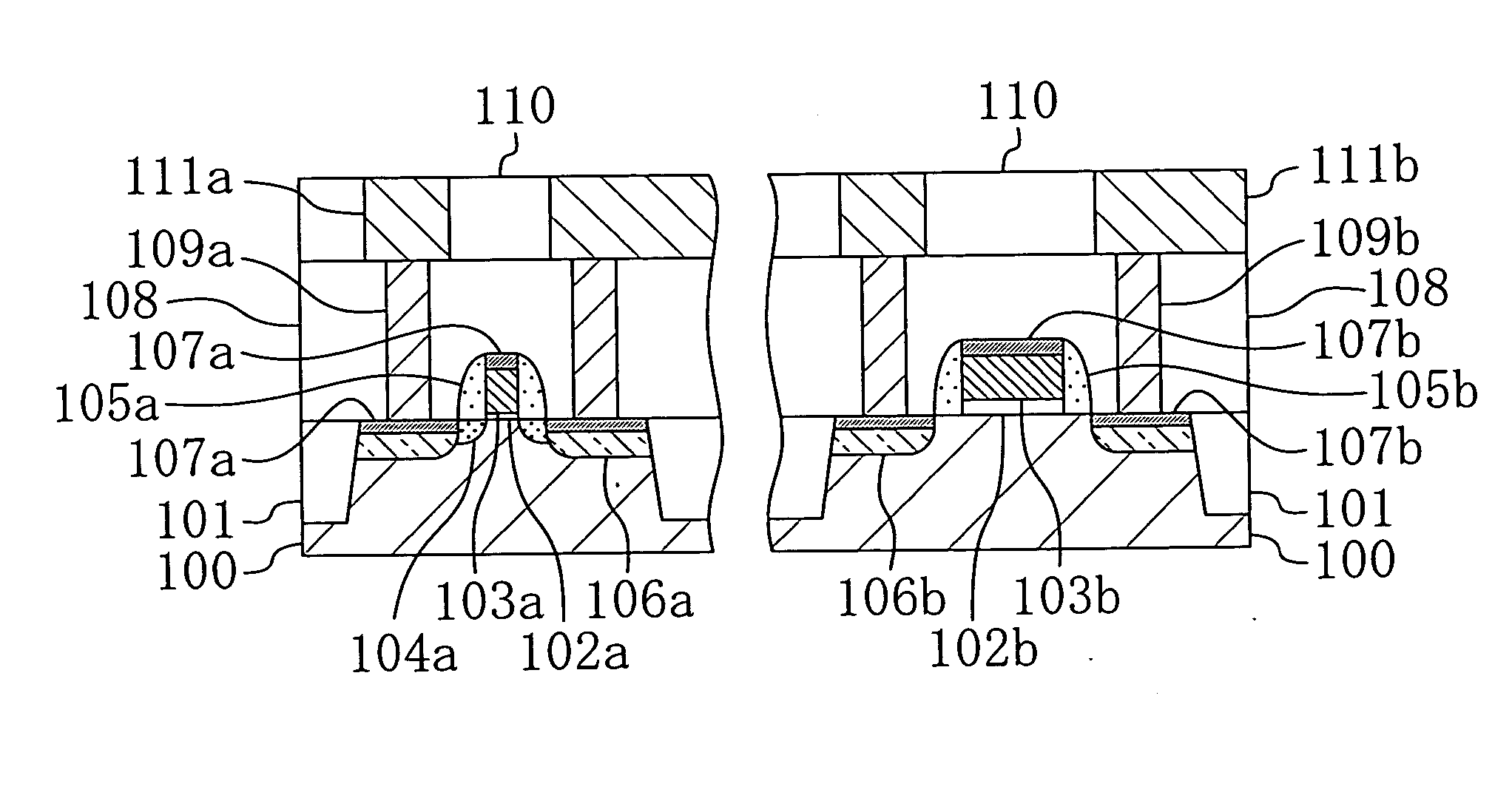
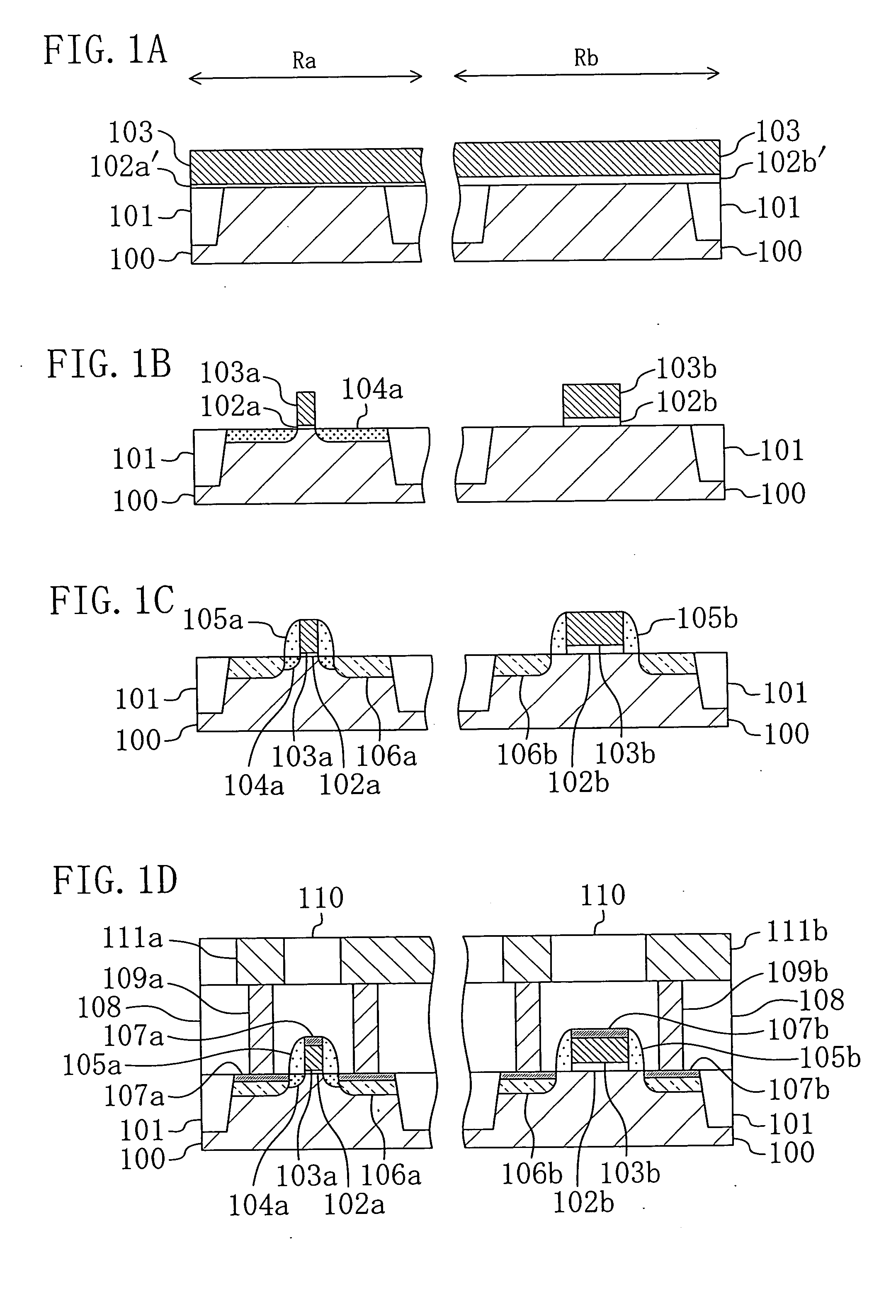
[0044]FIG. 1A to FIG. 1D are sections showing steps of the semiconductor device manufacturing method in a step sequence according to Embodiment 1 of the present invention. Wherein, in FIG. 1A to FIG. 1D, each region on the left side in the drawings indicates a core transistor formation region Ra where a core transistor is to be formed, and each region on the right side in the drawings indicates an I / O transistor formation region Rb where an I / O transistor is to be formed.
[0045] First, as shown in FIG. 1A, after an element isolation 101 made of an oxide film is formed in a semiconductor substrate 100 by an ordinary element isolation formation method, a silicon oxinitride film 102a′ having a film thickness of, for example, 2 nm is formed on the semiconductor substrate 100 in the core transistor region Ra. As well, a silicon oxinitride film 102b′ having a film...
embodiment 2
[0056] A semiconductor device manufacturing method according to Embodiment 2 of the present invention will be described below.
[0057]FIG. 4A to FIG. 4D are sections showing steps of the semiconductor device manufacturing method in a step sequence according to Embodiment 2 of the present invention. Wherein, in FIG. 4A to FIG. 4D, each region on the left side in the drawings indicates a core transistor formation region Ra where a core transistor is to be formed, and each region on the right side in the drawings indicates an I / O transistor formation region Rb where an I / O transistor is to be formed.
[0058] First, as shown in FIG. 4A, after an element isolation 101 made of an oxide film is formed in a semiconductor substrate 100 by an ordinary element isolation formation method, a silicon oxinitride film 102a′ having a film thickness of, for example, 2 nm is formed on the semiconductor substrate 100 in the core transistor region Ra. As well, a silicon oxinitride film 102c′ having a film...
embodiment 3
[0069] A semiconductor device manufacturing method according to Embodiment 3 of the present invention will be described below.
[0070]FIG. 5A to FIG. 5D are sections showing steps of the semiconductor device manufacturing method in a step sequence according to Embodiment 3 of the present invention. Wherein, in FIG. 5A to FIG. 5D, each region on the left side in the drawings indicates a core transistor formation region Ra where a core transistor is to be formed, and each region on the right side in the drawings indicates an I / O transistor formation region Rb where an I / O transistor is to be formed.
[0071] First, as shown in FIG. 5A, after an element isolation 101 made of an oxide film is formed in a semiconductor substrate 100 by an ordinary element isolation formation method, a silicon oxinitride film 102a′ having a film thickness of, for example, 2 nm is formed on the semiconductor substrate 100 in the core transistor region Ra. As well, a silicon oxinitride film 102d′ having a film...
PUM
 Abstract
Description
Claims
Application Information