Semiconductor device and manufacturing method thereof

a technology of semiconductor devices and manufacturing methods, applied in semiconductor devices, electrical devices, transistors, etc., can solve the problems of low low alignment distance high likelihood of misalignment etc., to achieve the effect of reducing the contact area between the gate electrode and the plug, reducing the upper surface area of the gate electrode, and reducing the gate electrode length

Inactive Publication Date: 2011-05-05
RENESAS ELECTRONICS CORP +1
View PDF3 Cites 6 Cited by
  • Summary
  • Abstract
  • Description
  • Claims
  • Application Information

AI Technical Summary

Benefits of technology

[0011]However, when the gate electrode is miniaturized, the gate length of the gate electrode is also shortened, and the area of the upper surface of the gate electrode is also decreased. Therefore, when the MISFET is miniaturized, the contact area between the gate electrode and the plug is decreased. This means that the contact resistance between the gate electrode and the plug is increased. Furthermore, when the area of the upper surface of the gate electrode is decreased, higher alignment accuracy of the gate electrode to the plug is required. As a result, when the gate electrode is miniaturized, the alignment margin between the gate electrode and the plug is reduced, and the misalignment between the gate electrode and the plug is likely to occur. In such a case, when the misalignment by the photolithography technology occurs, the gate electrode and the plug are not electrically connected, resulting in the connection failure. As described above, as the gate electrode is miniaturized, the improvement of the reliability in the electrical connection between the gate electrode and the plug is more required.
[0012]An object of the present invention is to provide a technology capable of improving the connection reliability between a gate electrode and a plug.

Problems solved by technology

As a result, when the gate electrode is miniaturized, the alignment margin between the gate electrode and the plug is reduced, and the misalignment between the gate electrode and the plug is likely to occur.
In such a case, when the misalignment by the photolithography technology occurs, the gate electrode and the plug are not electrically connected, resulting in the connection failure.

Method used


Image

  • Semiconductor device and manufacturing method thereof
  • Semiconductor device and manufacturing method thereof
  • Semiconductor device and manufacturing method thereof

Examples


first embodiment

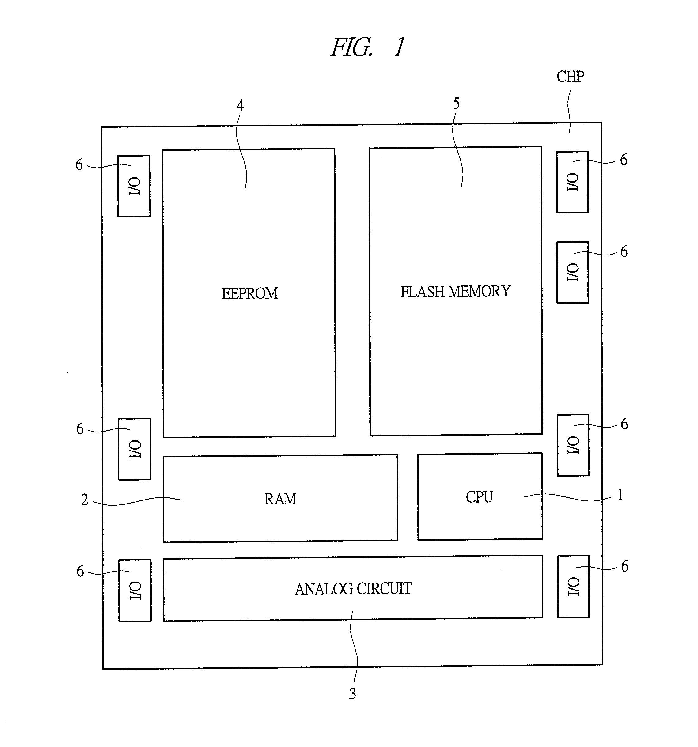
[0077]A semiconductor device according to the first embodiment will be described with reference to the drawings. First, a layout configuration of a semiconductor chip in which a system including a microcomputer is formed will be described. FIG. 1 is a diagram showing a layout configuration of a semiconductor chip CHP according to the first embodiment. In FIG. 1, the semiconductor chip CHP includes a CPU (Central Processing Unit) 1, a RAM (Random Access Memory) 2, an analog circuit 3, an EEPROM (Electrical Erasable Programmable Read Only Memory) 4, a flash memory 5 and I / O (Input / Output) circuits 6.

[0078]The CPU (circuit) 1 is also referred to as a central processing unit, and it corresponds to a heart of the computer or others. This CPU 1 reads and deciphers an instruction from a storage device and carries out various operations and controls based on the instruction.

[0079]The RAM (circuit) 2 is a memory in which the memory information can be accessed in a random manner, in other wor...

second embodiment

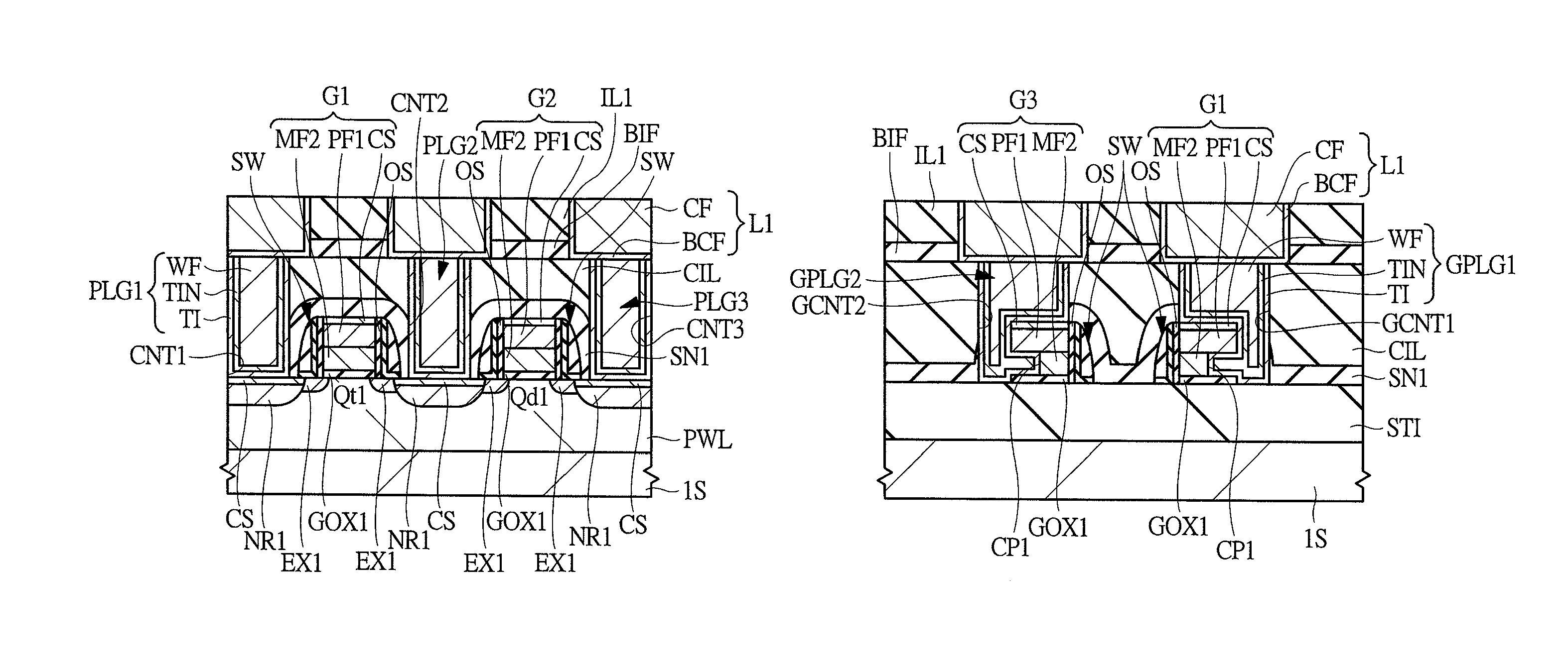
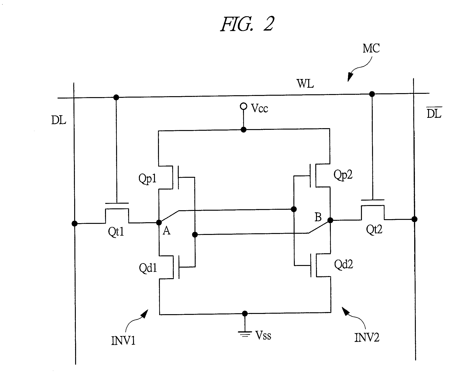
[0184]In the first embodiment, the structure of an n channel MISFET out of the MISFETs constituting a memory cell of an SRAM has been described, and furthermore, the characteristic connection structure between a gate electrode of the n channel MISFET and a gate plug has been described. In the second embodiment, the structure of a p channel MISFET out of the MISFETs constituting a memory cell of an SRAM will be described, and furthermore, the characteristic structure of a shared plug will be described. In the second embodiment, a cross-sectional view taken along the line C-C in FIG. 3 is used.

[0185]FIG. 24 is a cross-sectional view taken along the line C-C in FIG. 3. FIG. 24 shows the load MISFET Qp1 which is a p channel MISFET and the shared plugs SPLG1 and SPLG2.

[0186]First, the structure of the load MISFET Qp1 will be described. As shown in FIG. 24, the element isolation regions STI are formed in the semiconductor substrate 1S, and an n type well NWL is formed in the active region...

third embodiment

[0245]In the first embodiment, as shown in FIG. 4, for example, in the gate electrode G1 connected to the gate plug GPLG1 on the element isolation region STI, the concave portion CP1 is formed in one side surface of the metal film MF2 constituting a part of the gate electrode G1, thereby achieving the reduction of the parasitic resistance and the improvement of the connection reliability between the gate electrode G1 and the gate plug GPLG1. On the other hand, in the second embodiment, as shown in FIG. 24, in the shared plug SPLG1 which simultaneously connects the drain region of the load MISFET Qp1 and the gate electrode G4 formed on the element isolation region STI, the concave portion CP2 is formed in one side surface of the metal film MF2 constituting a part of the gate electrode G4 connected to the shared plug SPLG1. By this means, also in the second embodiment, the reduction of the parasitic resistance and the improvement of the connection reliability between the gate electrod...


PUM


Abstract

The present invention presupposes a MIPS electrode in which a gate electrode of a MISFET is made up of a stacked film of a metal film and a polysilicon film. Then, by a first characteristic point that a gate contact hole is formed to have an opening diameter larger than a gate length of the gate electrode of the MIPS electrode and a second characteristic point that a concave portion is formed in a side surface of the metal film constituting the gate electrode, the further reduction of the gate resistance (parasitic resistance) and the improvement of the connection reliability between the gate electrode and the gate plug can be achieved.

Description

CROSS-REFERENCE TO RELATED APPLICATION[0001]The present application claims priority from Japanese Patent Application No. 2009-250569 filed on Oct. 30, 2009, the content of which is hereby incorporated by reference to this application.TECHNICAL FIELD OF THE INVENTION[0002]The present invention relates to a semiconductor device and a manufacturing technology thereof, and more particularly to a technology effectively applied to a semiconductor device having a structure in which a plug is connected to a gate electrode of a MISFET (Metal Insulator Semiconductor Field Effect Transistor) and a manufacturing technology thereof.BACKGROUND OF THE INVENTION[0003]Japanese Patent Application Laid-Open Publication No. 11-340322 (Patent Document 1) discloses a technology relating to a shared contact of an SRAM (Static Random Access Memory). An object of this technology is to suppress the increase of the contact resistance caused by the removal of an upper conductive layer which appears first in a ...

Claims


Application Information

Patent Timeline
Patent Type & Authority Applications(United States)
IPC IPC(8): H01L27/088H01L21/336H01L29/78
CPCH01L21/76895H01L21/82385H01L27/1104H01L27/11H01L27/0207H10B10/00H10B10/12
Inventor TAKEUCHI, MASAHIKONAKAGAWA, RYONAKAGAWA, KAZUO
Owner RENESAS ELECTRONICS CORP
Why Eureka
Try Eureka