Mis transistor and cmos transistor

Inactive Publication Date: 2006-12-14
FOUND FOR ADVANCEMENT OF INT SCI
View PDF7 Cites 2 Cited by
  • Summary
  • Abstract
  • Description
  • Claims
  • Application Information

AI Technical Summary

Benefits of technology

[0024] With such a configuration, the channel generated along the gate insulator of the MIS transistor is generated along said at least two different crystal planes. In a MIS transistor with such a configuration, the channel width can be acquired in a direction different from a crystal plane, which directly enlarges the element area. It is possible to control the reduction of the amount of energy which is effective for driving a transistor, for each unit length of channel width in the channel generated along the gate insulator.
[0026] Such a configuration allows the control of reduction in the energy amount which is effective for driving a transistor, for each unit length of the channel width in the channel generated along the gate insulator.
[0027] Furthermore, by the generation of the channel along with the projecting part, it is possible to control the channel length modulation effect, which is reduction of the effective gate length and an increase in the drain current, caused by the shift of a pinch-off point (a point where the channel carrier density becomes approximately 0) in the saturation region in the transistor characteristics.
[0031] With such a configuration, in a p-channel MOS transistor, which is a direct cause of the large element area of the CMOS transistor, a gate insulator can be formed on a crystal plane oriented in a different direction from a crystal plane, which directly causes the element area of the CMOS transistor to be large. For that reason, in the p-channel MOS transistor, the channel width of a channel generated along the gate insulator can be generated in a different direction from a direction, which directly causes the element area to be large. Then, the current driving capacity of the p-channel MOS transistor and the current driving capacity of the n-channel MOS transistor can be matched without variation in element area between the MOS transistors.

Problems solved by technology

However, in a general configuration of an MIS transistor, it is difficult to enhance the integrity of elements on a semiconductor because the element area of the MIS transistor increases as the channel width increases.
Conversely, in the attempt to match the element areas, the channel widths become the same and thus the current driving capacities do not match.

Method used


Image

  • Mis transistor and cmos transistor
  • Mis transistor and cmos transistor
  • Mis transistor and cmos transistor

Examples


Embodiment Construction

[0046] In the following description, details of a preferred embodiment of the present invention are set forth with reference to the accompanying drawings.

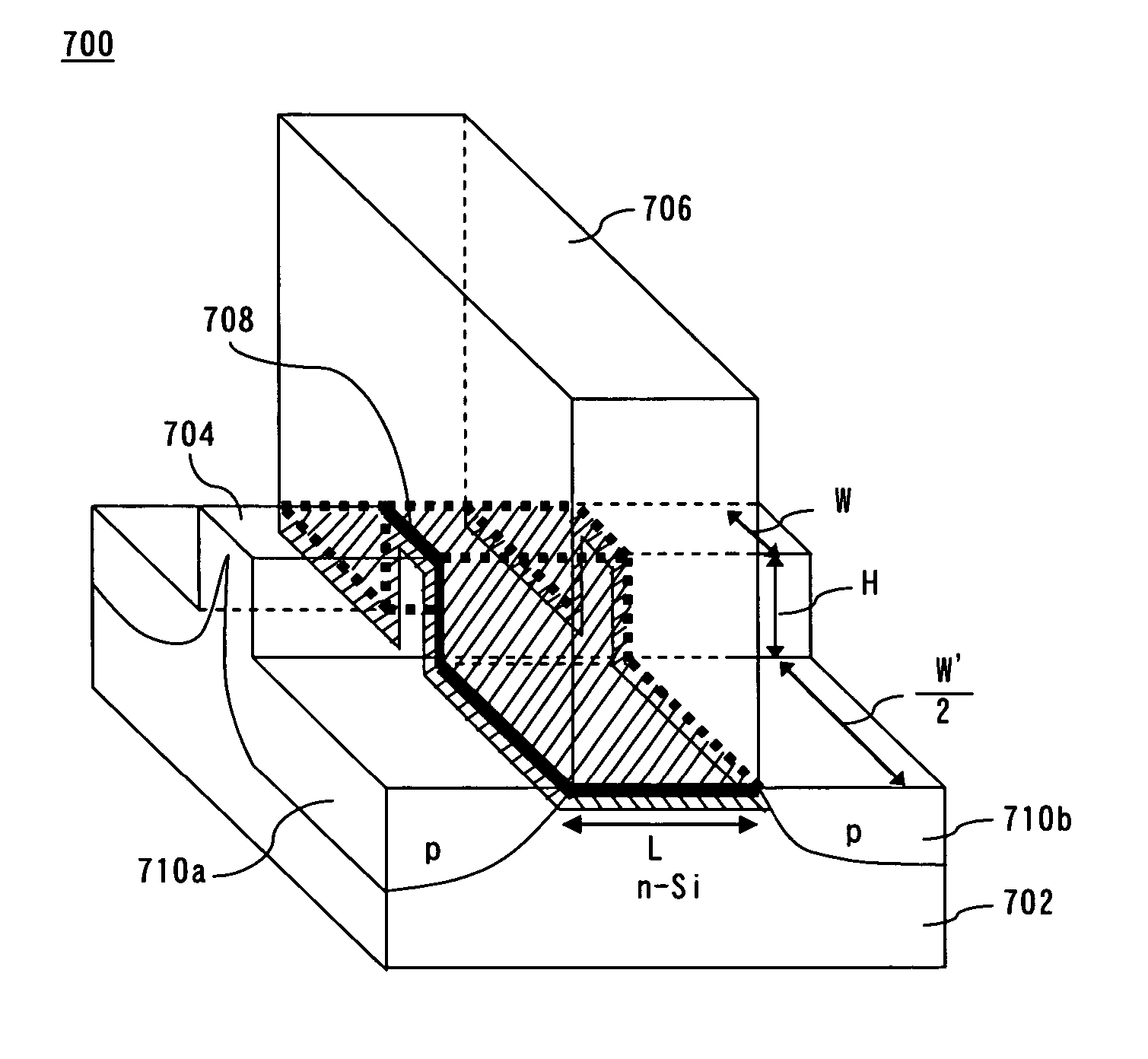
[0047] A transistor of the embodiment of the present invention has an MIS (Metal Insulator Semiconductor) configuration.

[0048] A gate insulator of the MIS transistor is formed based on a gate insulator thin film formation technique, in which a thin gate insulator of an MIS transistor is formed with high performance electrical characteristics, as disclosed in Japanese laid-open unexamined patent publication No. 2002-261091.

[0049] An explanation of the gate insulator thin film formation technique of the MIS transistor is provided first.

[0050] Regarding the type of gate insulator of the MIS transistor there are a variety such as an oxide film, a nitride film and an oxynitride film described in Japanese laid-open unexamined patent publication No. 2002-261091, and also many varieties for semiconductor substrates with different cryst...


PUM


Abstract

A MIS transistor, formed on a semiconductor substrate, assumed to comprise a semiconductor substrate (702, 910) comprising a projecting part (704, 910B) with at least two different crystal planes on the surface on a principal plane, a gate insulator (708, 920B) for covering at least a part of each of said at least two different crystal planes constituting the surface of the projecting part, a gate electrode (706, 930B), comprised on each of said at least two different crystal planes constituting the surface of the projecting part, which sandwiches the gate insulator with the said at least two different planes, and a single conductivity type diffusion region (710a, 710b, 910c, 910d) formed in the projecting part facing each of said at least two different crystal planes and individually formed on both sides of the gate electrode. Such a configuration allows control over increase in the element area and increase of channel width.

Description

TECHNICAL FIELD [0001] The present invention relates to a technology to adjust the gate width of an MIS (Metal Insulator Semiconductor) transistor. BACKGROUND ART [0002] The MIS (Metal Insulator Semiconductor) transistor is known as a semiconductor device from the past. [0003] There are various fabrication methods of a gate insulator comprised in a MIS transistor, and one example is the technique of thermal oxidation, which is thermal oxidation treatment at approximately 800° C. or above using oxygen molecules and water molecules. [0004] According to such a thermal oxidation technique, as a preprocess of the thermal oxidation process forming the gate insulator, processing to remove surface attached contaminants such as organic matter, metals and particles, followed by cleaning using diluted hydrofluoric acid and hydrogenated water, silicon dangling bonds on the surface of the silicon substrate (there are other semiconductor substrates such as germanium) on which the gate insulator i...

Claims


Application Information

Patent Timeline
IPC IPC(8): H01L29/94H01L21/8238H01L27/092H01L29/78
CPCH01L21/823807H01L21/823821H01L29/7851H01L21/823885H01L29/045H01L21/82385H01L21/18
Inventor NISHIMUTA, TAKEFUMIMIYAGI, HIROSHIOHMI, TADAHIROSUGAWA, SHIGETOSHITERAMOTO, AKINOBU
Owner FOUND FOR ADVANCEMENT OF INT SCI
Why Eureka
Try Eureka