Wafer processing method

Active Publication Date: 2005-12-22
DISCO CORP
View PDF18 Cites 47 Cited by
  • Summary
  • Abstract
  • Description
  • Claims
  • Application Information

AI Technical Summary

Benefits of technology

[0023] According to the wafer processing method in the present invention, the deteriorated layer formed along the dividing lines of the wafer by the deteriorated layer forming step is removed by carrying out the step of grinding the back surface to th

Problems solved by technology

Since the cutting blade has a thickness of about 20 μm, however, the dividing lines for sectioning chips must have a width of about 50 μm, and consequently, the area ratio of the dividing lines to the wafer is large, thereby reducing productivity.
Further, since a sapphire substrate, silicon carbide substrate, etc. have high Mohs hardness, cutting with th

Method used


Image

  • Wafer processing method
  • Wafer processing method
  • Wafer processing method

Examples


Embodiment Construction

[0041] Preferred embodiments of the present invention will be described in detail hereinunder with reference to the accompanying drawings.

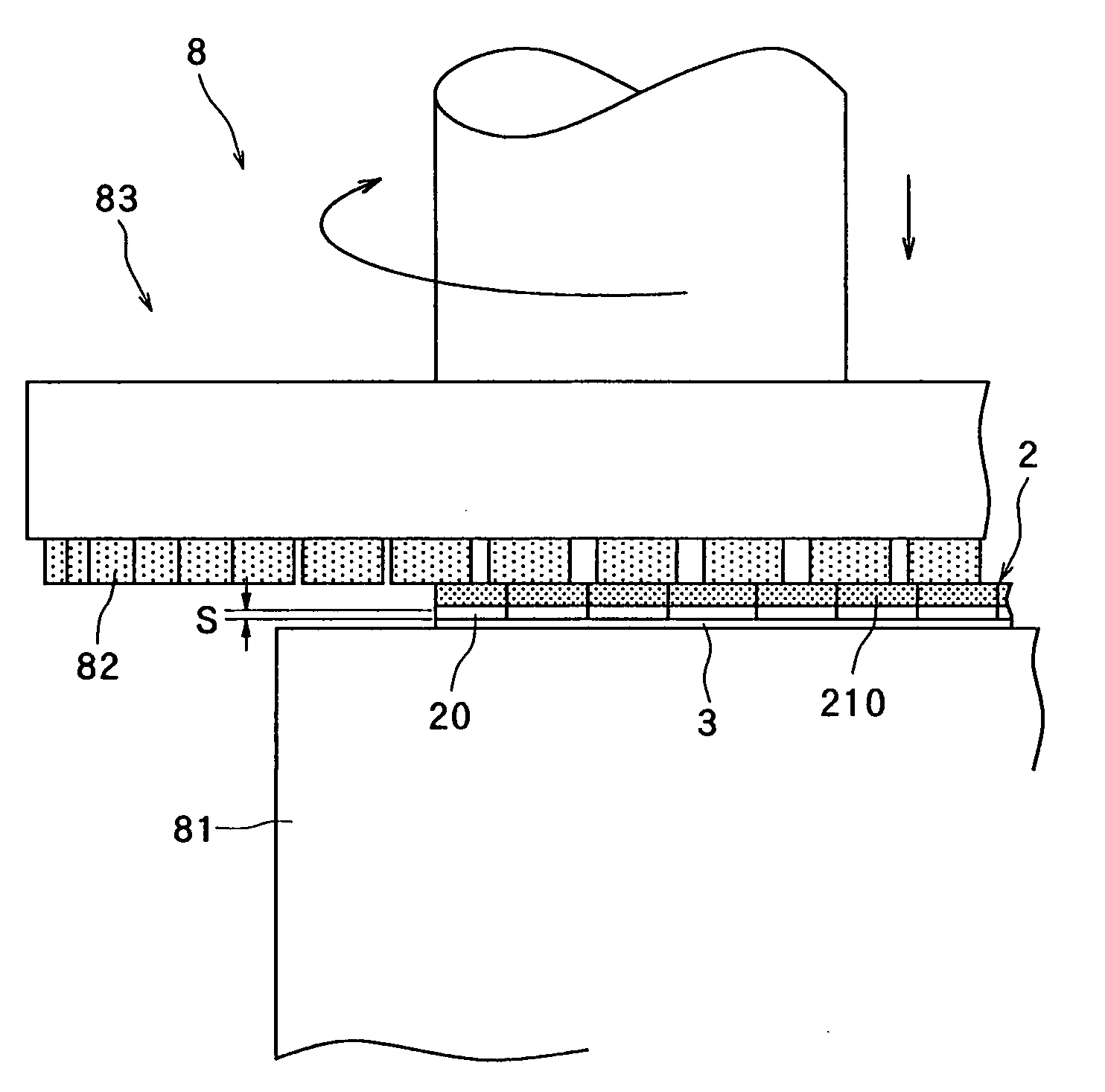
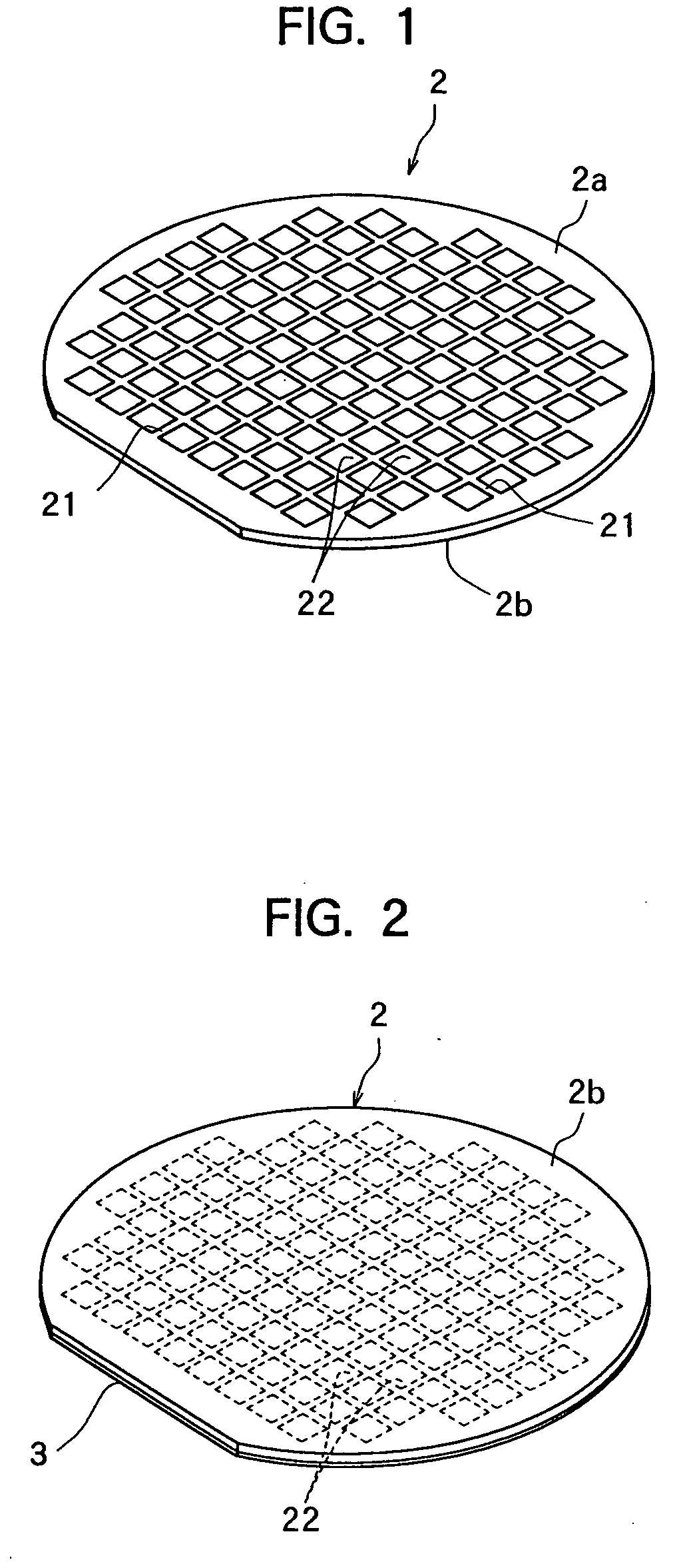
[0042]FIG. 1 is a perspective view of a semiconductor wafer as a wafer to be processed according to the present invention. The semiconductor wafer 2 shown in FIG. 1 is a silicon wafer with a thickness of, for example, 500 μm, which has a plurality of dividing lines 21 formed in a lattice pattern on the front surface 2a and circuits 22 formed as function elements in a plurality of areas sectioned by the plurality of dividing lines 21. A protective tape 3 is affixed to the front surface 2a of the thus constituted semiconductor wafer 2, as shown in FIG. 2 (protective tape affixing step).

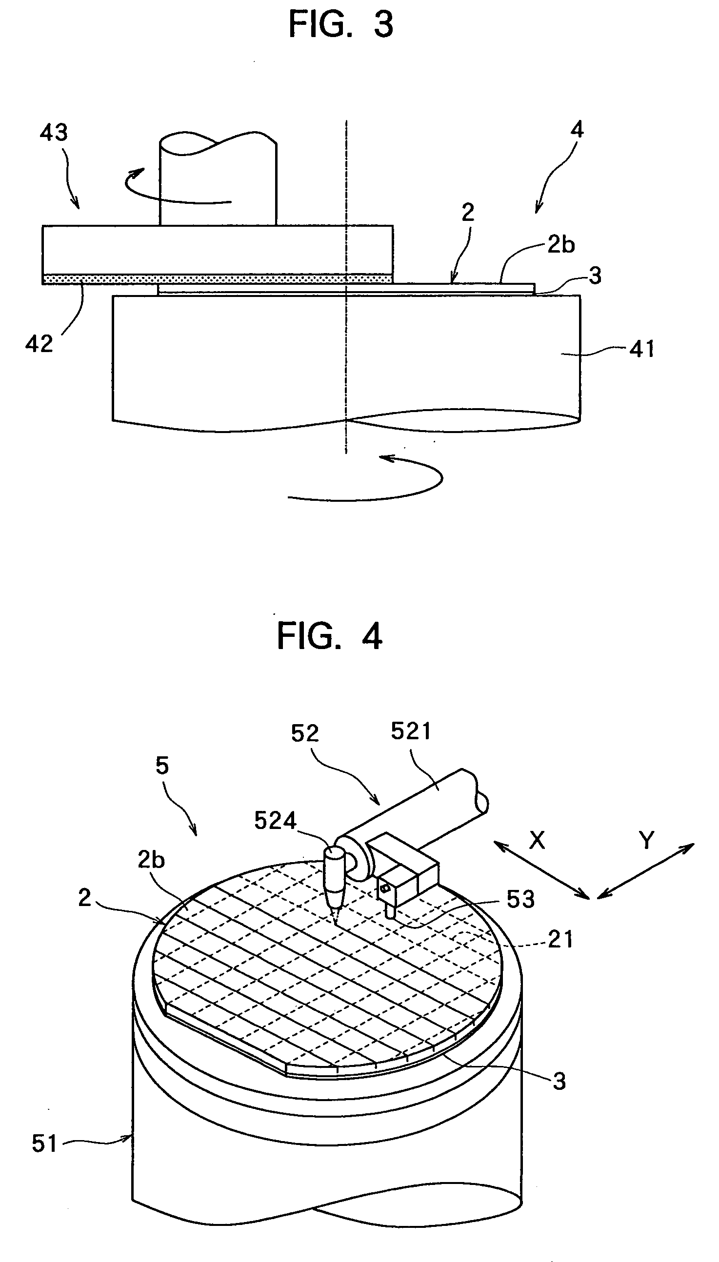
[0043] After the protective tape affixing step is carried out to affix the protective tape 3 to the front surface 2a of the semiconductor wafer 2, next comes a polish-processing step for grinding or polishing the back surface 2b of the semiconductor wafer 2 to form ...


PUM

PropertyMeasurementUnit
Fractionaaaaaaaaaa
Thicknessaaaaaaaaaa
Thermal stressaaaaaaaaaa

Abstract

A wafer processing method for dividing a wafer having function elements in area sectioned by dividing lines formed on the front surface in a lattice pattern into individual chips along the dividing lines, comprising a deteriorated layer forming step for forming a deteriorated layer on the side of the back surface of a position at a distance corresponding to the final thickness of the chip from the front surface of the wafer by applying a laser beam capable of passing through the wafer along the dividing lines from the back surface of the wafer; a dividing step for dividing the wafer into individual chips along the dividing lines by applying external force to the wafer in which the deteriorated layer has been formed along the dividing lines; and a back surface grinding step for grinding the back surface of the wafer divided into individual chips to the final thickness of the chip.

Description

FIELD OF THE INVENTION [0001] The present invention relates to a wafer processing method for dividing a wafer having function elements in areas sectioned by dividing lines formed on the front surface in a lattice pattern along the dividing lines. DESCRIPTION OF THE PRIOR ART [0002] In the production process of a semiconductor device, a plurality of areas are sectioned by dividing lines called “streets” arranged in a lattice pattern on the front surface of a substantially disk-like semiconductor wafer, and a circuit (function element) such as IC or LSI is formed in each of the sectioned areas. Individual semiconductor chips are manufactured by cutting this semiconductor wafer along the dividing lines to divide it into the areas having a circuit formed thereon. An optical device wafer comprising photodetectors (function elements) such as photodiodes or light-emitting elements (function elements) such as laser diodes laminated on the front surface of a sapphire substrate is also cut al...

Claims


Application Information

Patent Timeline
IPC IPC(8): B23K26/40B28D5/00H01L21/30H01L21/301H01L21/304H01L21/78
CPCB23K26/4075B28D5/0011H01L21/304B23K2201/40H01L2221/6834B23K26/0057H01L21/78B23K26/40B23K26/53B23K2101/40B23K2103/50
Inventor NAGAI, YUSUKEKOBAYASHI, SATOSHINAKAMURA, MASARU
Owner DISCO CORP
Why Eureka
Try Eureka