Semiconductor display device and electronic appliance

a display device and semiconductor technology, applied in semiconductor devices, electrical appliances, instruments, etc., can solve the problems of increasing the drive frequency and more pseudo-contours in the pixel portion, so as to increase the number of gray scales, secure the writing period, and suppress the drive frequency of the driver circuit.

Active Publication Date: 2005-12-29
SEMICON ENERGY LAB CO LTD
View PDF11 Cites 31 Cited by
  • Summary
  • Abstract
  • Description
  • Claims
  • Application Information

AI Technical Summary

Benefits of technology

[0022] Thus, the length of the writing period can be secured even when the number of sub-frame periods appearing in one frame period is increased, thereby the drive frequency of a driver circuit can be suppressed while increasing the number of gray scales. Further, even when the sub-frame period is further divided into a plurality of periods, the length of the writing period can be secured, thereby the drive frequency of a driver circuit can be suppressed while suppressing the generation of pseudo-contours.
[0023] Note that the time gray scale method includes a Simultaneously-Erasing-Scan (SES) method in addition to the DPS method. According to the SES method, a sub-frame period is made shorter than a writing period by forming a transistor for forcibly stopping a current supply to a light-emitting element in each pixel, and providing a period in which the pixels do not emit light (non-display period). In the case of the light-emitting device of the invention, the non-display period can be made shorter as compared to the SES method, or eliminated ultimately. Therefore, the duty ratio (ratio of the periods used for controlling gray scales which occupy one frame period) can be increased. Accordingly, the power consumption of the pixel portion can be suppressed while enhancing the contrast of a displayed image. Further, according to the invention, the number of transistors provided in each pixel can be suppressed as compared to the SES method. Accordingly, in the case of a bottom-emission light-emitting device in which light emitted from light-emitting elements travels in the direction of the transistors, the aperture ratio of pixels (ratio of the areas through which light can be extracted) can be increased.
[0024] In addition, as one of the time gray scale methods, there is a driving method in which a row writing period is divided in half, the first half of the row writing period (first row writing period) is used for writing video signals to pixels, and the second half of the row writing period (second row

Problems solved by technology

However, taking into account the reliability of the driver circuit, it is not preferable to increase the drive frequency much.
Further, the time gray sca

Method used


Image

  • Semiconductor display device and electronic appliance
  • Semiconductor display device and electronic appliance
  • Semiconductor display device and electronic appliance

Examples


embodiment 1

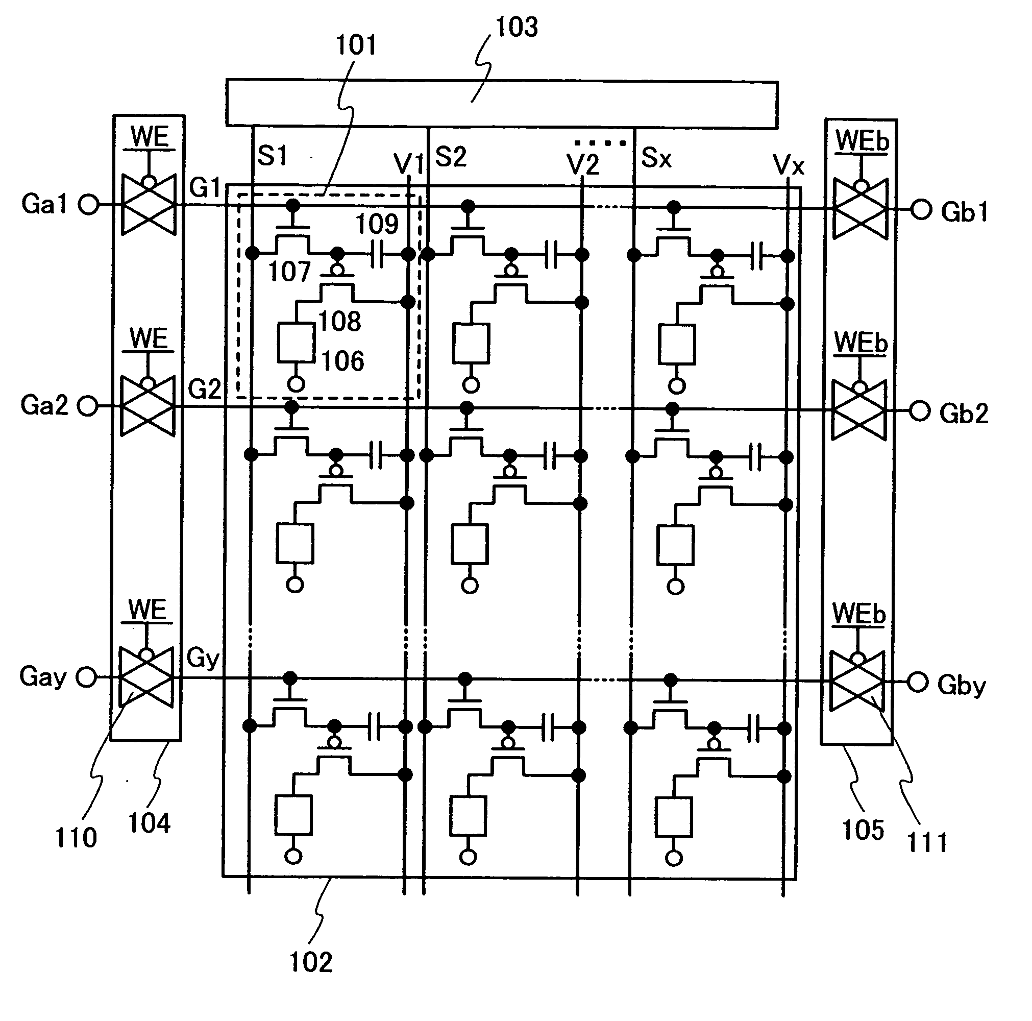
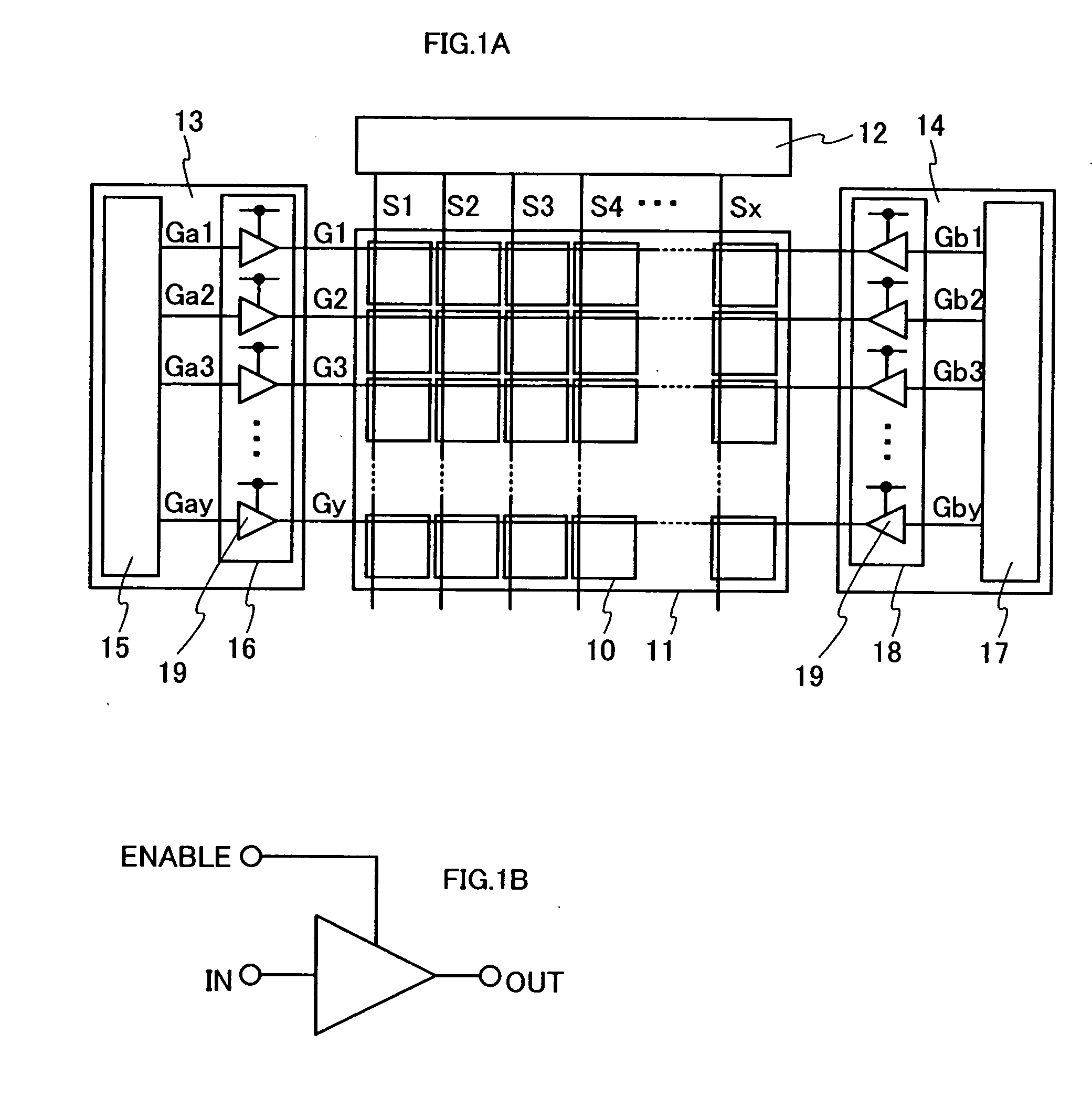
[0070] In this embodiment, description is made on a configuration of a driver circuit used in the semiconductor display device of the invention. FIG. 7 is a block diagram of the semiconductor display device of the invention. The semiconductor display device shown in FIG. 7 includes a pixel portion 200 where a plurality of pixels each having a display element such as a light-emitting element and a liquid crystal element are formed, first and second scan line driver circuits 201 and 202 for selecting each pixel, and a signal line driver circuit 203 for controlling an input of video signals to the selected pixel.

[0071] In FIG. 7, the signal line driver circuit 203 includes a shift register 204, a first latch 205, and a second latch 206. The shift register 204 is inputted with clock signals SCK for signal lines, and start pulse signals SSP for the signal lines. Upon input of the clock signals SCK and the start pulse signals SSP, the shift register 204 generates timing signals. The gene...

embodiment 2

[0079] In this embodiment, description is made in further detail on the operation of the signal line driver circuit 203 shown in FIG. 7. FIG. 8A is a block diagram of the signal line driver circuit 203. As described in Embodiment 1, the signal line driver circuit 203 includes the shift register 204, the first latch 205, and the second latch 206. The shift register 204 is inputted with clock signals SCK, start pulse signals SSP, and inverted clock signals SCKb. The first latch 205 is inputted with video signals, and the second latch 206 is inputted with latch signals LP. Video signals inputted to the first latch 205 in a serial manner are inputted to the signal lines S1 to Sx in a parallel manner from the second latch 206.

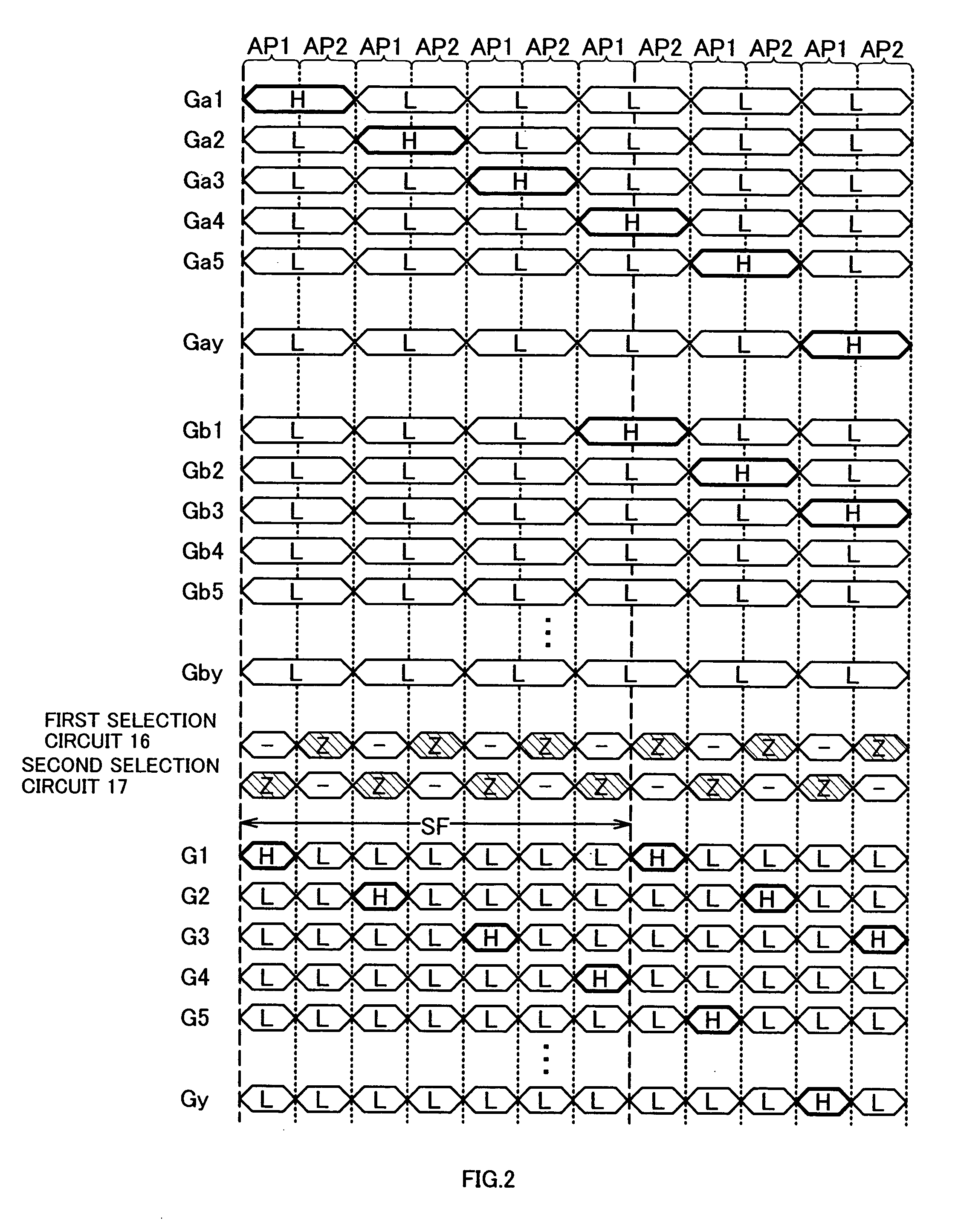
[0080]FIG. 8B is a timing chart of the signal line driver circuit 203 shown in FIG. 8A. In synchronization with a start pulse signal SSP, a serial video signal having the data of Daj which corresponds to the pixels in the j-th row is written to the first latch 205....

embodiment 3

[0089] In this embodiment, description is made with reference to FIGS. 9A to 9C on the sectional structure of a pixel in the case where a P-channel driving transistor is employed. Note that FIGS. 9A to 9C each illustrates the case where a first electrode is an anode while the second electrode is a cathode; however, the first electrode may be a cathode while the second electrode may be an anode.

[0090]FIG. 9A is a sectional diagram of a pixel in the case where a P-channel transistor is used as a driving transistor 6001, and light emitted from a light-emitting element 6003 is extracted from a first electrode 6004.

[0091] The driving transistor 6001 is covered with an interlayer insulating film 6007, over which a bank 6008 having an opening portion is formed. In the opening portion of the bank 6008, the first electrode 6004 is partially exposed, and the first electrode 6004, an electroluminescent layer 6005, and a second electrode 6006 are stacked in this order.

[0092] The interlayer i...


PUM


Abstract

A semiconductor display device which can suppress the drive frequency while increasing the number of gray scales. According to the semiconductor display device, a plurality of pixels can be selected per row by a first scan line driver circuit, the plurality of pixels can be selected per row by a second scan line driver circuit, writing of a first video signal to the row selected by the first scan line driver circuit is controlled by a signal line driver circuit, writing of a second video signal to the row selected by the second scan line driver circuit is controlled by the signal line driver circuit, and using respective selection circuits included in the first and second scan line driver circuits, the output from the second scan line driver circuit to the plurality of pixels can be set at high impedance while the row is selected by the first scan line driver circuit, or the output from the first scan line driver circuit to the plurality of pixels can be set at high impedance while the row is selected by the second scan line driver circuit.

Description

BACKGROUND OF THE INVENTION [0001] 1. Field of the Invention [0002] The present invention relates to a semiconductor display device for displaying images by a time gray scale method. In addition, the invention relates to an electronic appliance using the semiconductor display device. [0003] 2. Description of the Related Art [0004] As a driving method of a light-emitting device which is one of the semiconductor display devices, there is a time gray scale method for displaying gray scales by controlling the emission period of pixels using a binary voltage value of a digital video signal. Generally, electroluminscent materials exhibit high response in comparison with liquid crystals; therefore, the light-emitting device is more suitable for the time gray scale method. Specifically, in the case of displaying images by the time gray scale method, one frame period is divided into a plurality of sub-frame periods. In accordance with video signals, pixels are controlled to emit light or no ...

Claims


Application Information

Patent Timeline
IPC IPC(8): G09G3/30
CPCG09G3/20G09G3/2022G09G3/3208H01L27/3244G09G2300/0842G09G2310/02G09G2310/0267G09G2300/08H10K59/12
Inventor IWABUCHI, TOMOYUKI
Owner SEMICON ENERGY LAB CO LTD
Why Eureka
Try Eureka